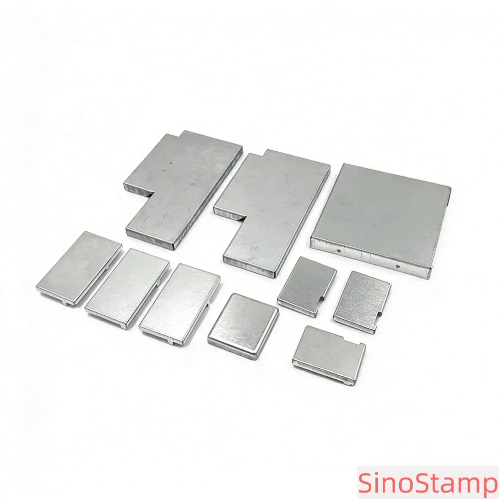
EMI shielding covers are important metal components used in electronic products to help reduce electromagnetic interference (EMI) and radio frequency interference (RFI). As electronic devices become smaller, faster, and more functionally integrated, controlling unwanted electromagnetic emissions and susceptibility has become an important consideration in electronic product design. Custom metal shielding covers provide a practical solution for protecting sensitive circuit areas, communication modules, and electronic assemblies from electromagnetic interference.
SinoStamp supplies custom EMI shielding covers for OEM manufacturers, electronic component companies, PCB assemblers, and industrial product developers. Our product range focuses on precision stamped metal covers manufactured according to customer drawings, samples, dimensions, and technical specifications. Depending on the application, available material options include tinplate, stainless steel, copper, and nickel silver.
We support customized shapes, dimensions, material thicknesses, mounting structures, openings, surface finishes, and forming requirements. Our manufacturing solutions can involve precision blanking, punching, bending, forming, and dedicated tooling development according to the component design and production quantity.
Whether you need a simple shielding cover for a compact electronic board or a customized metal enclosure for a more complex RF module, selecting the correct material, structure, manufacturing process, and installation method is essential. SinoStamp works with OEM customers to evaluate component requirements and coordinate suitable metal stamping solutions for prototype development and repeat production.
EMI shielding covers are conductive metal structures designed to help control electromagnetic interference around sensitive electronic components or circuit sections. They are commonly installed over selected areas of a printed circuit board (PCB), communication module, RF circuit, or other electronic assembly.
Electronic circuits can generate electromagnetic energy during normal operation. High-frequency signals, switching components, wireless communication circuits, and digital processing systems may create unwanted electromagnetic emissions. External electromagnetic fields can also interfere with sensitive electronic circuits and affect their operation.
A properly designed shielding cover can help reduce electromagnetic coupling by providing a conductive barrier around the protected area. Its effectiveness depends on several factors, including material properties, cover geometry, wall height, openings, seams, grounding arrangements, contact pressure, and the complete installation structure.
Metal EMI shielding covers are generally manufactured from conductive sheet materials and formed into shapes that match the electronic assembly. They may include flat surfaces, sidewalls, mounting tabs, retaining features, openings, and other customized structures.
Unlike a standard protective housing, an EMI shielding cover must be considered as part of the electromagnetic design of the final product. The metal material alone does not determine shielding performance. Electrical continuity, grounding contact, aperture dimensions, and assembly interfaces also play important roles.
OEM electronic products often have different circuit layouts, installation spaces, operating frequencies, and mechanical requirements. As a result, standard shielding covers may not always fit the customer's design. Custom EMI shielding covers allow manufacturers to specify the dimensions, shape, material, thickness, and structural features required by their electronic assemblies.
SinoStamp supports customized metal shielding components based on engineering drawings, CAD files, physical samples, and customer specifications. The manufacturing approach is evaluated according to the part geometry, material characteristics, tolerance requirements, and expected production volume.
Shielding covers can be manufactured in different lengths, widths, heights, and profiles. The dimensions should correspond to the available PCB space and the electronic components that need to be protected.
Customers can specify overall dimensions, wall heights, corner structures, mounting positions, and other critical measurements. For compact electronic assemblies, dimensional accuracy is particularly important because a small variation may affect installation clearance or the contact between the cover and the supporting structure.
Different circuit layouts require different shielding structures. Common designs include rectangular covers, square covers, low-profile shielding covers, multi-sided enclosures, and customized formed metal structures.
Depending on the application, the cover may include rounded corners, folded edges, sidewalls, tabs, slots, and other structural details. These features can be incorporated into the stamping and forming process according to the approved design.
Some electronic shielding covers require openings for connectors, cables, adjustment components, ventilation, or other assembly features. The position and dimensions of these openings should be carefully evaluated because openings can influence electromagnetic shielding performance.
OEM customers can provide drawings showing the required cutouts and mounting features. Our engineering review can consider whether the proposed structure is suitable for the selected manufacturing process and whether any design adjustments should be evaluated before tooling development.
Shielding covers may use solderable tabs, mounting flanges, retaining clips, folded edges, or other mechanical structures to connect with the PCB or supporting assembly.
The correct structure depends on the installation method, electrical grounding requirements, mechanical stability, and product assembly process. Mounting features should be defined clearly in the technical drawing to help maintain consistent production results.
EMI shielding covers can be designed in different structural forms according to the electronic product and the protected circuit area. The most suitable design depends on the required shielding arrangement, available installation space, maintenance requirements, and manufacturing considerations.
One-piece shielding covers are manufactured as a single metal structure. They may include a top surface, sidewalls, and formed mounting features integrated into the same component.
This design can provide a compact structure with fewer separate components. It is suitable for electronic assemblies where the shielding cover does not need frequent removal for maintenance or adjustment.
Depending on the geometry, one-piece covers may be manufactured through blanking, bending, forming, and other precision stamping operations. The tooling design should consider the forming sequence and the required dimensional relationships between the top surface and sidewalls.
Some electronic shielding systems use a combination of a metal frame and a removable cover. The frame is installed on the PCB, while the upper cover can be removed when inspection, repair, or component replacement is required.
This structure can be useful for products requiring maintenance access or engineering adjustments during development. The frame and cover must be designed to provide suitable mechanical engagement and electrical contact.
For this type of assembly, the frame geometry, cover fit, retention structure, and contact arrangement should be evaluated together rather than as independent metal components.
Low-profile shielding covers are designed for compact electronic products where vertical installation space is limited. They may be used in wireless modules, portable electronics, communication devices, and densely populated PCB assemblies.
Low-profile structures require careful control of overall height, wall geometry, and forming dimensions. The design should also consider clearance between the cover and the electronic components underneath it.
Some electronic assemblies contain multiple circuit sections that need to be separated or shielded individually. Multi-compartment shielding structures can provide separate metal partitions within a common shielding arrangement.
These designs may include internal walls, partitions, different chamber dimensions, and multiple mounting features. Manufacturing complexity depends on the number of compartments, material thickness, forming depth, and required tolerances.
For multi-compartment designs, OEM engineers should consider the electromagnetic behavior of the complete assembly, including internal connections, openings, grounding, and the positioning of electronic components.
Material selection is an important part of EMI shielding cover development. Different metals offer different electrical conductivity, magnetic properties, corrosion resistance, mechanical strength, formability, and surface characteristics.
The correct material should be selected according to the operating frequency, shielding design, installation environment, forming requirements, and total product cost. SinoStamp supports several commonly used sheet metal materials for customized shielding cover projects.
Tinplate is a steel-based sheet material with a tin coating. It is used in certain electronic shielding applications because it combines a steel substrate with a conductive surface finish and can be processed into a range of stamped metal structures.
Tinplate shielding covers may be suitable for applications where material cost, forming characteristics, and surface properties need to be balanced. The selected tin coating and substrate specifications should be confirmed according to the customer's requirements.
During manufacturing, material thickness, coating condition, forming geometry, and edge quality should be considered. Excessive deformation or unsuitable processing conditions may affect the surface coating, so the manufacturing process should be evaluated for the specific design.
Stainless steel is selected for applications requiring corrosion resistance, mechanical strength, and structural stability. It is available in different grades with different mechanical and forming properties.
Stainless steel shielding covers can be used in industrial electronics, communication equipment, appliance electronics, and other assemblies where durability and environmental resistance are important.
Because stainless steel generally has lower electrical conductivity than copper, its suitability for a particular shielding application should be evaluated according to the electromagnetic design. Grounding and contact arrangements may also require special attention.
Copper is widely recognized for its excellent electrical conductivity. It is used in electronic and electrical applications where conductive properties are important.
Copper shielding covers may be suitable for selected RF and electronic shielding designs. Its relatively soft mechanical characteristics can influence tooling design, handling, and forming operations.
When selecting copper, OEM buyers should specify the required copper grade and material condition where applicable. The manufacturer should consider the forming requirements, dimensional stability, and surface protection needs of the finished component.
Nickel silver is a copper-based alloy that typically contains nickel and zinc. Despite its name, it does not contain silver. It is used in selected electronic and precision metal component applications because of its useful combination of mechanical properties, appearance, and corrosion characteristics.
Nickel silver shielding covers may be considered when the application requires a particular balance of conductivity, strength, forming behavior, and surface characteristics.
The exact alloy composition and material grade should be confirmed before production. Different grades can have different electrical and mechanical properties, which may affect the final component design.
When comparing materials for EMI shielding covers, OEM engineers should evaluate several factors:
There is no single material that is ideal for every shielding application. The best choice depends on the complete electronic assembly and the required performance. Where shielding effectiveness is critical, material selection should be supported by design evaluation and testing of the finished assembly.
Material thickness affects the mechanical properties, forming behavior, weight, dimensional stability, and manufacturing cost of an EMI shielding cover. A suitable thickness should provide sufficient structural stability while fitting the available space and manufacturing requirements.
Thin-gauge materials are frequently considered for compact electronic shielding applications because they can help reduce component weight and installation height. However, very thin materials may be more sensitive to deformation, handling damage, and dimensional variation.
Thicker materials may provide greater rigidity, but they can require different tooling conditions and more forming force. The selected thickness should therefore be evaluated together with the part dimensions, wall height, corner geometry, and mounting arrangement.
SinoStamp supports customized material thickness according to the component design and manufacturing feasibility. The final specification should be confirmed after reviewing the technical drawing, material grade, and required production process.
Important dimensions for EMI shielding covers may include overall length, width, height, wall position, mounting tab location, opening dimensions, and the distance between functional features.
Not every dimension requires the same tolerance. OEM engineers should identify critical-to-function dimensions that affect PCB installation, mechanical fit, grounding contact, or assembly performance.
Achievable tolerances depend on material properties, thickness, part geometry, tooling design, forming sequence, and inspection methods. A realistic tolerance specification helps avoid unnecessary tooling complexity and manufacturing costs.
Before production, the supplier and customer should agree on the drawing revision, inspection method, critical dimensions, and sample approval criteria.
The manufacturing process for an EMI shielding cover depends on its geometry, material, thickness, and production quantity. Precision stamping provides a practical way to manufacture repeatable metal components with customized profiles and forming features.
Blanking is used to cut the basic outline of a metal component from sheet or strip material. The blanking operation establishes the initial profile that will be used for subsequent forming operations.
For EMI shielding covers, the blanking layout should consider the required overall dimensions, material utilization, edge quality, and the position of future bending features.
Punching creates holes, slots, openings, and other internal features in metal components. These features may be required for mounting, fastening, connector clearance, or other assembly purposes.
Hole position and size should be controlled according to the engineering drawing. For shielding applications, openings should also be considered in relation to the electromagnetic requirements of the complete assembly.
Bending transforms a flat metal blank into a three-dimensional structure. It is commonly used to create sidewalls, flanges, mounting tabs, and folded edges on shielding covers.
Material thickness, bend radius, material direction, and springback should be considered during tooling development. These factors influence the final dimensions and the fit of the finished cover.
Forming operations are used to create specific shapes and structural features beyond simple flat cutting and bending. Depending on the design, forming may be used to produce raised sections, embossed features, retaining structures, or other customized geometries.
The forming sequence should be planned to reduce unnecessary material stress and maintain dimensional consistency.
Progressive die stamping integrates multiple stamping operations into a single die. A metal strip moves through different stations, with each station performing a defined cutting or forming operation.
This approach may be suitable for shielding covers with repeated features and stable production demand. It can reduce manual handling between operations and support efficient repeat production after tooling development and process stabilization.
Custom shielding covers often require dedicated tooling to achieve the specified dimensions and structural features. Tooling design should consider material properties, die clearance, forming sequence, dimensional requirements, and production volume.
Before tooling development, OEM customers should provide the latest engineering drawings, material specifications, and expected order quantities. The manufacturer can then evaluate the design and discuss the proposed manufacturing approach.
Tooling ownership, maintenance responsibilities, trial production arrangements, and modification costs should be clarified before the project begins. These details are particularly important for overseas customers planning long-term repeat production.
Surface finishing can influence the corrosion resistance, appearance, electrical contact behavior, solderability, and storage stability of EMI shielding covers. The appropriate treatment depends on the base material and the functional requirements of the electronic assembly.
Bright tin plating provides a bright metallic surface finish and is used in selected electronic and electrical component applications. It may be considered where surface appearance, solderability, and contact characteristics are relevant.
The plating specification should identify the required coating thickness and any applicable performance requirements. Coating adhesion and appearance should be checked after the manufacturing and finishing processes.
Matte finishes are selected when a non-glossy surface appearance is preferred. Depending on the material and process, matte surfaces may be produced through different finishing or coating arrangements.
OEM customers should specify the expected surface appearance and any functional requirements rather than relying only on a general finish description.
Anti-tarnish treatments may be used for selected metal surfaces to reduce discoloration during storage and handling. This can be relevant for components that require stable appearance or surface condition before assembly.
The suitability of a treatment should be confirmed against the base material, coating system, and final application. Buyers should also clarify storage conditions and the expected protection period.
Gold plating may be specified for selected electronic contact applications where particular contact and corrosion characteristics are required. It is not automatically necessary for every EMI shielding cover.
When gold plating is required, the coating thickness, underlayer, coverage area, and functional requirements should be clearly defined. The cost and manufacturing process depend on the specific plating specification.
Deburring removes or reduces sharp edges and unwanted burrs created during stamping. Proper edge treatment can improve handling safety, assembly compatibility, and the overall quality of the finished component.
For shielding covers, edge condition may also influence the mechanical fit and contact between mating surfaces. Acceptance criteria should be defined according to the part function and drawing requirements.
EMI shielding performance is an important design consideration for metal shielding covers. A conductive enclosure can help reduce electromagnetic coupling, but the final performance depends on more than the material itself.
Shielding effectiveness is commonly expressed in decibels (dB). It describes the reduction in electromagnetic field strength or power under specified test conditions. The measured result depends on frequency, test configuration, material properties, enclosure geometry, and installation conditions.
Electrical conductivity influences how electromagnetic currents are distributed across a conductive shielding structure. Copper offers high electrical conductivity, while stainless steel and other materials have different electrical and mechanical characteristics.
However, conductivity alone does not determine the final shielding effectiveness. The structure, grounding, openings, and contact interfaces must also be considered.
The size and shape of a shielding cover influence how it interacts with electromagnetic fields. Wall height, corner structure, aperture dimensions, and enclosure continuity may all affect performance.
Large openings, gaps, and discontinuities can create leakage paths. The design should consider the protected frequency range and the dimensions of any openings or seams.
Grounding is a critical part of many shielding arrangements. The cover may need to make electrical contact with a PCB ground structure, metal frame, or another conductive surface.
Mounting tabs, soldered joints, spring contacts, and conductive interfaces can be used depending on the assembly design. The contact arrangement should be defined during product development and verified in the final assembly.
Shielding effectiveness should be evaluated using a defined test method and frequency range. A material-level test does not necessarily represent the performance of the complete shielding cover after installation.
For applications with strict EMI or RF requirements, OEM customers should consider testing the finished assembly under representative operating and installation conditions. The test method, equipment, frequency range, and acceptance criteria should be agreed upon before testing.
SinoStamp focuses on manufacturing metal shielding components according to customer drawings and specifications. Actual EMI or RF shielding performance must be verified through appropriate design evaluation and testing of the finished product or assembly. We do not assume a universal shielding value based only on the material or component appearance.
EMI shielding covers are used in a wide range of electronic products where electromagnetic compatibility and circuit protection are important. The required structure and material depend on the electronic system, operating environment, and installation method.
Printed circuit boards often contain multiple electronic components operating at different frequencies and signal levels. Metal shielding covers can be installed over selected circuit areas to help control interference between circuit sections and external sources.
PCB shielding designs may include one-piece covers, removable covers, frames, and custom partitions. The correct structure depends on board layout, component height, grounding arrangements, and assembly requirements.
WiFi modules operate using radio frequency signals and may be installed in products containing other digital or wireless circuits. Custom metal shielding structures can help manage electromagnetic coupling within compact electronic assemblies.
Cover dimensions, openings, grounding points, and installation clearances should be reviewed according to the module design.
Bluetooth modules are commonly integrated into consumer electronics, industrial devices, and communication products. Depending on the system design, shielding covers may be used to help isolate sensitive circuit sections or manage interference between components.
RF communication systems may contain sensitive signal-processing and transmission circuits. Metal shielding covers can form part of the electromagnetic compatibility strategy for these assemblies.
The shielding structure should be designed according to the operating frequency, enclosure configuration, antenna arrangement, and grounding requirements.
Portable devices, smart home products, audio equipment, and other electronic products may use customized shielding components to manage interference in compact assemblies.
These applications often require small dimensions, lightweight structures, precise forming, and compatibility with automated PCB assembly.
Industrial electronic equipment may operate in environments with electrical switching devices, motors, communication systems, and other potential sources of interference.
Custom shielding covers can be incorporated into control boards, communication modules, and electronic assemblies where electromagnetic compatibility is part of the product design.
Consistent quality is essential for custom metal shielding components because dimensional variations and surface defects can affect installation, contact, and assembly performance.
A suitable quality control process should cover incoming materials, tooling trials, in-process production, finishing, and final inspection.
Incoming inspection may include checking material grade documentation, thickness, width, surface condition, and batch identification. The inspection requirements should reflect the customer's material specification.
First article inspection verifies that the initial stamped components meet the approved engineering drawing. Important dimensions may include overall size, wall height, opening location, mounting features, and formed geometry.
Where required, the manufacturer can prepare dimensional inspection records for customer review before mass production approval.
During stamping production, inspection may include dimensional checks, visual examination, burr assessment, and monitoring of process conditions. The inspection frequency should be determined according to product complexity, production volume, and quality requirements.
Final inspection may cover dimensions, surface appearance, edge condition, forming quality, plating condition, and packaging. Additional functional or assembly checks may be required for selected projects.
OEM buyers may require inspection reports, material certificates, production batch identification, or other quality documentation. These requirements should be agreed upon before production so the manufacturer can establish suitable records and procedures.
Quality acceptance criteria should be based on approved drawings, agreed specifications, and applicable testing methods rather than general descriptions such as perfect quality or high precision.
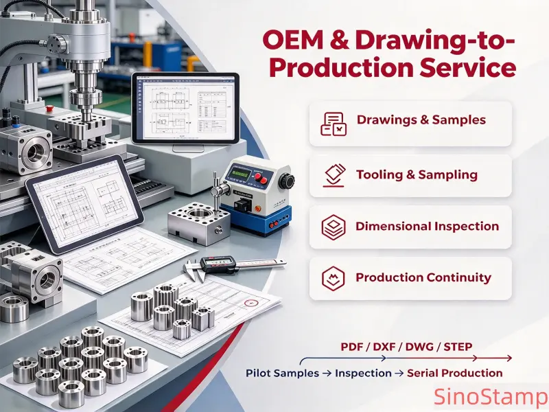
Custom EMI shielding cover projects usually begin with a technical drawing, sample, or electronic assembly requirement. The manufacturer then evaluates the design, material, forming operations, and tooling requirements before preparing a manufacturing proposal.
SinoStamp supports OEM and ODM customization for metal shielding components according to customer project requirements.
Customers can provide 2D drawings, 3D CAD files, or other technical documentation. These documents help define the component dimensions, material requirements, tolerances, surface finishes, and installation features.
Where a technical drawing is not available, customers may provide an existing component sample for evaluation. The sample can help identify the overall geometry and manufacturing requirements. Additional measurements or engineering information may still be necessary before tooling development.
Different materials and production methods may be suitable for the same general component design. The manufacturing solution should balance technical requirements, formability, dimensional accuracy, tooling investment, and production quantity.
Sample production allows OEM customers to evaluate dimensions, fit, appearance, and assembly compatibility before approving regular production. The sample development process may involve tooling trials and design adjustments where necessary.
For long-term OEM projects, approved drawings, material specifications, tooling conditions, and inspection requirements should be maintained consistently. Clear documentation helps reduce variation between repeat orders and supports ongoing product supply.
When sourcing EMI shielding covers from China, OEM buyers should evaluate the supplier's manufacturing experience, engineering communication, material knowledge, tooling capabilities, quality control, and ability to support repeat production.
Ask whether the supplier has manufactured similar electronic shielding components. Experience with thin-gauge metal, small stamped parts, forming operations, and electronic assembly requirements can be valuable for customized projects.
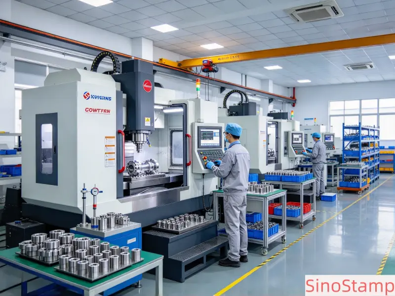
Review the supplier's available stamping processes, tooling development arrangements, production equipment, and ability to handle the required material thickness and part geometry.
Ask how the supplier measures critical dimensions, controls burrs, inspects surface finishes, and handles nonconforming products. Where required, request sample inspection reports and relevant quality documentation.
Make sure the supplier understands the required material grade, thickness, plating type, and coating requirements. Material substitutions or changes to surface treatments should be approved before production.
For small and medium-sized OEM companies, the ability to support samples, pilot production, and repeat orders is important. Discuss expected quantities and annual demand so the supplier can evaluate an appropriate tooling and production arrangement.
A reliable supplier should respond clearly to technical questions, identify potential manufacturing risks, and provide realistic schedules for tooling, samples, production, and shipment.
Providing complete technical information helps the manufacturer evaluate the project and prepare a more accurate quotation. Before requesting a quotation, OEM buyers should prepare the following details whenever possible:
For projects with specific EMI or RF performance requirements, buyers should also provide the target frequency range, applicable shielding test method, grounding arrangement, and any available test data. These details help the manufacturer understand the role of the metal component within the complete assembly.
SinoStamp focuses on custom metal stamping components for international OEM customers. Our approach is based on understanding customer drawings and technical requirements, evaluating practical manufacturing solutions, and coordinating production according to approved specifications.
We support customized dimensions, shapes, material thicknesses, openings, mounting features, and surface finishing requirements. Each project is evaluated according to the actual component design rather than relying only on standard product dimensions.
Depending on the application, customers can specify tinplate, stainless steel, copper, nickel silver, or other suitable materials. Material selection should be confirmed according to the required electrical, mechanical, environmental, and forming characteristics.
Manufacturing processes can include blanking, punching, bending, forming, and other suitable stamping operations. The selected process depends on component geometry, material thickness, tolerance requirements, and expected production volume.
We work with OEM customers based on engineering drawings, physical samples, and technical specifications. Our project evaluation can cover material options, tooling requirements, manufacturing processes, sample development, and repeat production planning.
SinoStamp is focused on supplying custom metal components to overseas industrial and electronic customers. Clear technical communication, quotation details, production coordination, and agreed inspection requirements are important parts of our cooperation approach.
Our goal is to support customers seeking a practical China-based sourcing solution for customized EMI shielding covers and other precision metal stamping components.
EMI shielding covers are important components in electronic product design because they help control electromagnetic interference around sensitive circuit areas. Their effectiveness depends on the correct combination of material properties, cover geometry, grounding, contact interfaces, openings, and final assembly conditions.
For OEM manufacturers, selecting a suitable shielding cover requires more than choosing a metal material. Dimensions, thickness, forming structure, surface finishing, tooling design, and inspection requirements must all be considered during product development.
Custom metal stamping provides flexible manufacturing options for different shielding structures, from simple covers to more complex formed components. Progressive die stamping or separate stamping operations may be selected according to the component design and expected production volume.
SinoStamp supports customized EMI shielding covers for electronic applications, including PCB assemblies, WiFi modules, Bluetooth modules, RF communication systems, and industrial electronics. We welcome customer drawings, samples, and technical requirements for manufacturing evaluation.
If you are looking for a China-based EMI shielding covers supplier for your OEM project, prepare your product drawings, material specifications, required dimensions, surface finish, and estimated order quantity. These details will help us evaluate the project and discuss a suitable custom metal stamping solution.
```