SinoStamp is a China-based manufacturer and supplier of custom electronic metal stamping parts for electronics manufacturers, PCB assembly companies, communication equipment producers, and industrial electronics brands. We specialize in manufacturing precision stamped metal components according to customer drawings, engineering specifications, physical samples, and OEM project requirements. Our product range includes EMI shielding covers, PCB shielding cans, electronic metal brackets, battery contact components, and electronic spring contacts. We support customized manufacturing projects from initial design evaluation and sample development to tooling coordination and repeat production.
Electronic products continue to become smaller, more integrated, and more functionally complex. As a result, the demand for precision metal components with controlled dimensions, stable forming characteristics, and consistent material properties continues to grow. Electronic metal stamping provides an efficient manufacturing solution for producing thin metal parts used in electromagnetic shielding, electrical connections, internal support structures, and mechanical fastening. These components may appear relatively simple, but their dimensions and material characteristics can directly influence the assembly accuracy and operating performance of the finished electronic product.
For OEM manufacturers, selecting the right electronic metal stamping supplier involves more than comparing unit prices. Buyers need to evaluate manufacturing feasibility, material selection, tooling arrangements, dimensional consistency, surface finishing, production capacity, and communication throughout the project. SinoStamp focuses on custom B2B manufacturing and works with customers to understand their technical requirements before production. Whether you are sourcing a small shielding cover for a PCB assembly or developing a series of custom metal contacts for an electronic device, we aim to provide a practical manufacturing solution that matches your product specifications and purchasing requirements.
Electronic metal stamping is widely used to manufacture components that require precise shapes, repeatable dimensions, and efficient production. The process transforms sheet metal or metal strip into finished components through operations such as blanking, piercing, bending, forming, and drawing. Depending on the part geometry and production quantity, different tooling arrangements can be selected to achieve the required component structure.
Our custom manufacturing service is designed for customers who need non-standard metal components rather than generic hardware products. We can evaluate projects based on 2D engineering drawings, 3D CAD models, existing samples, or detailed product specifications. Important manufacturing considerations include material grade, thickness, component dimensions, tolerance requirements, bend geometry, hole positions, surface finishing, and final assembly conditions.
For new electronic product development, early manufacturing evaluation can help identify potential issues before production tooling is completed. For example, a shielding cover may require specific wall heights and contact structures to fit a PCB assembly. A battery contact may require controlled spring characteristics and a suitable conductive material. An electronic mounting bracket may need precise hole positions to maintain alignment with other internal components. Reviewing these requirements before production helps establish a more reliable manufacturing process.
We support OEM customers developing new components as well as companies looking for an alternative supplier for existing electronic metal parts. Depending on the product design and order quantity, manufacturing arrangements may include prototype samples, custom tooling, small-batch production, and ongoing repeat orders. Our objective is to help customers establish a consistent supply arrangement for their electronic metal stamping requirements.
SinoStamp organizes its electronic metal stamping product range around five main product categories. Each category serves different functions within electronic equipment and requires specific considerations during material selection, tooling development, and quality inspection. By focusing on these product applications, we can better understand the manufacturing requirements of electronic equipment manufacturers and provide more relevant support during project evaluation.
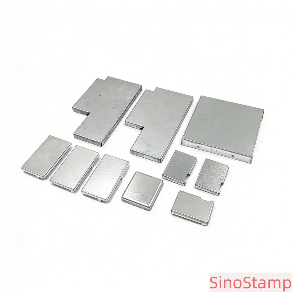
EMI shielding covers are metal components designed to help reduce electromagnetic interference within electronic devices and assemblies. They are commonly used in wireless communication modules, RF circuits, networking equipment, computer hardware, control boards, and other electronic products containing sensitive components. A shielding cover forms a conductive enclosure around selected circuits or components, helping control unwanted electromagnetic coupling between different sections of an electronic system.
Custom EMI shielding covers can be manufactured in different shapes and configurations depending on the electronic assembly. Common designs include rectangular covers, square shielding enclosures, formed metal caps, multi-compartment covers, and custom-shaped shielding structures. Some products use a one-piece design, while others consist of a separate metal frame and removable cover. The most suitable construction depends on the PCB layout, installation method, inspection requirements, and product design.
Material selection is an important consideration when developing EMI shielding covers. Tinplate, nickel silver, stainless steel, and other suitable conductive sheet materials may be considered depending on shielding requirements, forming characteristics, corrosion resistance, and cost. Material thickness also affects rigidity, forming behavior, and dimensional stability. Engineers should evaluate the required material and thickness based on the intended frequency range and overall shielding design rather than relying on material conductivity alone.
The manufacturing process may include blanking, piercing, bending, forming, and additional surface treatment. Dimensional accuracy is particularly important around the cover edges, mounting features, and contact areas. Improper forming or excessive deformation can affect installation and the quality of the connection between the shielding cover and the corresponding PCB structure.
It is important to understand that the actual shielding effectiveness of an EMI shielding cover depends on the complete assembly. Factors such as enclosure openings, seams, grounding connections, contact pressure, installation gaps, and PCB layout can influence the final electromagnetic performance. For projects with defined shielding targets, OEM customers should provide relevant performance specifications and assembly information for evaluation. Testing the complete electronic assembly may be necessary to verify the required shielding performance.
SinoStamp supports custom EMI shielding cover manufacturing according to customer drawings and samples. Customers can discuss material specifications, wall height, cover dimensions, mounting structures, surface finishing, and packaging requirements during the quotation stage. For new designs, prototype samples can help evaluate dimensional fit and installation compatibility before final production tooling is approved.
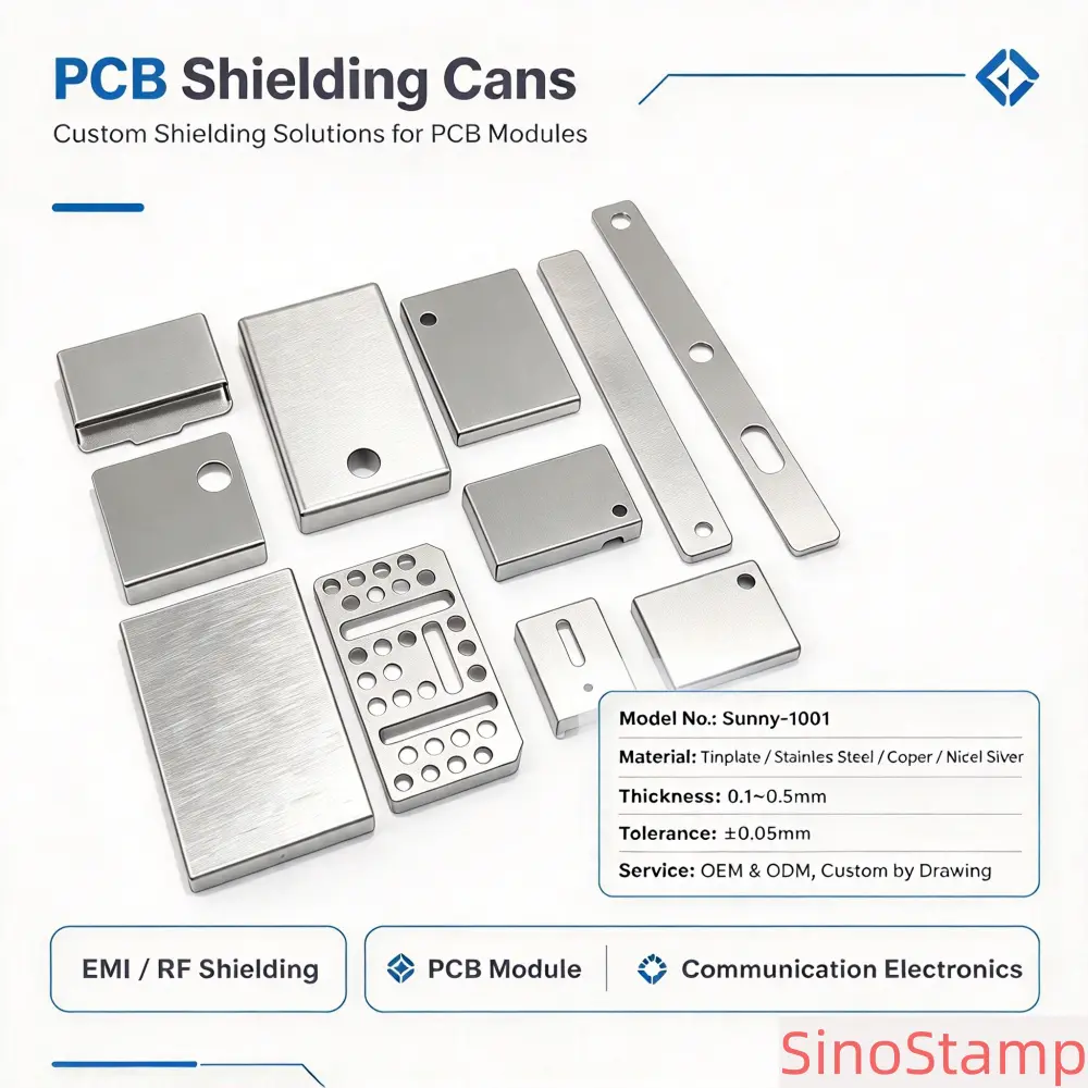
PCB shielding cans are precision metal components installed on printed circuit boards to isolate selected electronic circuits or components. They are commonly used in RF modules, wireless communication devices, GPS equipment, networking products, consumer electronics, and other compact electronic assemblies. Depending on the design, a PCB shielding can may consist of a single metal cover or a combination of a shielding frame and a removable lid.
Shielding cans are designed to fit specific PCB layouts, component heights, and installation requirements. Their dimensions must be coordinated with the circuit board structure and the electronic components located inside the shielding area. Important design features may include overall length and width, wall height, corner geometry, cover profile, contact points, and mounting details. Even relatively small dimensional deviations can affect installation compatibility and assembly efficiency.
Common materials for PCB shielding cans include tinplate, stainless steel, nickel silver, and other suitable metal sheets. Material selection depends on conductivity, formability, mechanical strength, corrosion resistance, and the intended shielding application. Some customers may specify a particular material grade or surface treatment based on their electronic product design and assembly process.
Manufacturing processes may involve precision blanking, piercing, bending, forming, and finishing. For shielding structures with narrow walls or small corner radii, tooling design and forming sequence are important factors. The production process should maintain the required shape without excessive distortion or damage to the contact surfaces. For multi-piece designs, the relationship between the frame and removable cover must also be considered.
PCB shielding cans are frequently supplied to manufacturers that operate automated PCB assembly lines. Therefore, dimensional consistency, packaging, and component handling are important purchasing considerations. Components should be protected against deformation, contamination, and surface damage during transportation and storage. Customers can specify packaging quantities and protection requirements according to their assembly procedures.
We manufacture custom PCB shielding cans based on customer drawings, 3D models, and physical samples. During project evaluation, we consider the required geometry, material thickness, forming operations, surface finish, and assembly conditions. For new product development, sample production provides an opportunity to verify the fit between the shielding structure and the PCB before regular manufacturing begins.
Electronic metal brackets are structural components used to support, secure, position, and connect assemblies inside electronic equipment. They are commonly found in communication devices, control systems, industrial electronics, computer hardware, display equipment, networking products, and electronic enclosures. Their main functions include providing mounting points, maintaining component alignment, reinforcing internal structures, and supporting mechanical connections.
Custom electronic brackets can have simple flat geometries or more complex shapes incorporating several bends, holes, slots, tabs, and formed sections. The design depends on the dimensions and mounting requirements of the components being supported. Some brackets are used to secure printed circuit boards, while others support displays, connectors, internal panels, power modules, or electronic housings.
Common material options include stainless steel, cold-rolled steel, galvanized steel, aluminum, and other sheet metals. The selection depends on required strength, weight, corrosion resistance, appearance, and manufacturing cost. Material thickness and structural geometry should be considered together because formed sections, bends, and reinforcement features can influence the overall stiffness of the finished bracket.
The manufacturing process may include blanking, piercing, bending, forming, deburring, and surface finishing. Hole position and bend angle are particularly important when brackets are designed for precise assembly. If the bracket is connected to multiple components, dimensional variations may create alignment problems or increase assembly time. Tooling and inspection requirements should therefore focus on the critical features identified in the engineering drawing.
For OEM customers, custom electronic metal brackets can be manufactured according to existing drawings or new product development specifications. We support project evaluation based on part geometry, material grade, thickness, tolerance requirements, and expected production quantity. Customers can also provide samples from existing products when developing replacement components or transferring production to a new supplier.
Battery contact components are conductive metal parts used to establish electrical connections between batteries and electronic devices. They are widely used in battery holders, portable electronic equipment, wireless accessories, remote controls, measurement devices, industrial control products, and other battery-powered systems. Depending on the product structure, these components may include positive and negative terminals, contact plates, spring contacts, and specially formed connection elements.
Battery contact components must combine suitable electrical conductivity with appropriate mechanical characteristics. The material should provide stable contact performance while maintaining the required shape during installation and use. Copper, brass, phosphor bronze, and other suitable conductive alloys may be considered according to the product design. Material selection should also consider hardness, elasticity, corrosion resistance, and the expected operating environment.
Some battery contact designs use a flat stamped terminal, while others incorporate a flexible spring section that maintains pressure against the battery surface. The geometry of the contact area, spring length, thickness, and forming angle can influence contact force and installation behavior. If the product requires repeated battery insertion and removal, the contact design should also consider mechanical durability and repeated operating cycles.
Surface finishing may be required to improve corrosion resistance or provide suitable contact characteristics. Common finishing specifications may include nickel plating, tin plating, or other treatments defined by the customer. The appropriate finish depends on the battery type, operating environment, electrical requirements, and product design.
SinoStamp supports custom battery contact component manufacturing according to engineering drawings and samples. Customers should provide information about battery dimensions, contact configuration, required material, surface treatment, and expected mechanical performance. These details help determine suitable stamping operations and material specifications before production begins.
Electronic spring contacts are precision stamped components designed to provide flexible electrical connections within electronic assemblies. They are used in battery systems, connectors, circuit boards, communication devices, switches, wireless equipment, and other electronic products requiring spring-loaded contact structures. Their function is to maintain a stable contact interface while accommodating the mechanical movement or dimensional variation of connected components.
Spring contact components are generally manufactured from materials with suitable elastic and conductive properties. Common material options include phosphor bronze, brass, stainless steel, and other spring-grade alloys. Copper alloys are often considered when electrical conductivity is a major requirement, while stainless steel may be suitable for certain mechanical spring applications. The final material should be selected according to the required spring force, electrical characteristics, fatigue behavior, and corrosion resistance.
The geometry of an electronic spring contact has a significant influence on its mechanical performance. Important features include material thickness, spring length, contact radius, forming angle, and the shape of the flexible section. These dimensions affect deflection, contact force, and the available movement range. For components with tight functional requirements, the spring structure should be evaluated during the design and sample development stages.
Precision stamping processes can produce spring contacts with repeatable shapes and consistent production dimensions. Depending on the design, manufacturing may involve blanking, piercing, bending, forming, and additional finishing operations. Tooling must be designed to control the forming process and reduce unwanted deformation. Material handling and production conditions are also important because spring characteristics can be affected by material properties and forming history.
We support custom electronic spring contact manufacturing based on customer drawings, specifications, and approved samples. OEM customers can provide the intended application, contact configuration, material requirements, and mechanical performance targets for evaluation. For new projects, sample testing can help confirm the fit and spring behavior before moving into regular production.
Material selection is one of the most important decisions in electronic metal stamping. Different electronic components have different requirements for electrical conductivity, mechanical strength, spring characteristics, corrosion resistance, weight, and forming behavior. A material that is suitable for a shielding cover may not be the best option for a battery contact or spring terminal. Therefore, material selection should be based on the actual function and technical specifications of each component.
Stainless steel is commonly used for electronic brackets, shielding structures, retaining clips, and other components requiring mechanical strength and corrosion resistance. Different stainless steel grades provide different forming and mechanical properties. The selected grade should be suitable for the component geometry and the intended operating environment. Material thickness and forming conditions should also be reviewed during tooling development.
Tinplate and tin-coated steel are used in selected electronic shielding applications because of their practical forming characteristics and conductive metal surface. They may be suitable for shielding covers, PCB shielding cans, and other formed metal enclosures. The suitability of a particular tin-coated material depends on thickness, coating characteristics, corrosion requirements, and the complete shielding design.
Copper and copper alloys are widely used for electronic contact components because of their electrical conductivity and formability. Typical applications include battery contacts, terminals, connector contacts, and conductive spring components. Brass and phosphor bronze are frequently considered for different combinations of conductivity and mechanical performance. The appropriate alloy depends on the contact function, required hardness, forming geometry, and surface finishing specifications.
Aluminum is used for electronic brackets and selected structural components where low weight and corrosion resistance are important. Its forming behavior differs from steel and copper alloys, so the alloy and temper should be considered when developing complex stamped shapes. Customers should provide the required material specification or application details for proper evaluation.
Material thickness affects component strength, rigidity, forming behavior, and finished dimensions. Thin materials may be suitable for compact shielding structures and contact components, while thicker materials may be necessary for mounting brackets and structural supports. The appropriate thickness depends on the part design and functional requirements. Critical dimensions and tolerances should be clearly identified in customer drawings to support tooling design and inspection planning.
The manufacturing process for electronic metal stamping parts depends on the geometry, material, thickness, dimensional requirements, and expected order quantity. Different products may require different combinations of cutting, forming, and finishing operations. Choosing an appropriate process can help improve dimensional consistency, production efficiency, and manufacturing cost.
Blanking and piercing are used to produce the external profile and internal openings of stamped components. They are commonly used for shielding covers, electronic brackets, contact plates, battery terminals, and spring contacts. Tooling clearance, cutting conditions, and material thickness influence the quality of the cut edges and the formation of burrs. For precision components, the required edge condition and dimensional tolerances should be defined before production.
Bending and forming operations transform flat sheet metal into three-dimensional shapes. These processes are essential for manufacturing shielding enclosures, mounting brackets, contact structures, and spring components. Material thickness, bend radius, grain direction, and springback can affect the final geometry. The tooling design and forming sequence should be evaluated according to the part structure and required dimensions.
Progressive die stamping is suitable for certain electronic components manufactured in repeated production quantities. Metal strip passes through multiple stations within a progressive die, with each station performing a specific operation. The finished component is produced after the material moves through the required sequence. This method can be effective for suitable small metal contacts, terminals, clips, and other components with repeat demand.
Progressive tooling requires careful consideration of strip layout, material utilization, part geometry, and production volume. For projects with relatively low quantities or frequently changing designs, alternative tooling methods may be more practical. The best manufacturing arrangement should be determined according to the customer's product requirements and expected purchasing schedule.
Custom tooling is a critical part of electronic metal stamping because the die determines the geometry and repeatability of the finished component. Depending on the design, tooling may include blanking dies, piercing dies, bending dies, compound dies, and progressive dies. The selection depends on the complexity of the component, material properties, production quantity, and required dimensional accuracy.
For new projects, customers can provide 2D drawings, 3D CAD files, or physical samples for manufacturing evaluation. Important design considerations include material thickness, critical dimensions, forming angles, hole positions, spring structures, and contact features. These details help determine the appropriate tooling structure and production sequence.
Before final tooling development, OEM customers should confirm the latest approved engineering drawings and material specifications. Any changes to dimensions, material, or functional requirements after tooling completion may affect manufacturing cost and development schedules. Clear communication during the design review stage can reduce unnecessary changes and improve the transition from prototype samples to production.
Surface finishing may be required to improve corrosion resistance, electrical contact characteristics, appearance, or compatibility with the customer's assembly process. The appropriate finishing method depends on the material and intended application. Electronic components may require different surface treatments from structural brackets because their electrical and mechanical functions are different.
Nickel plating may be specified for selected electronic contacts and metal components to provide surface protection and particular functional characteristics. Its suitability depends on the base material, required coating thickness, operating environment, and customer specifications. For electrical applications, the final contact performance should be evaluated according to the actual product requirements.
Tin plating is commonly specified for certain electrical and electronic components, including terminals and conductive contacts. It may provide useful solderability and surface protection characteristics in suitable applications. Coating thickness, coverage, base material, and environmental requirements should be clearly defined in the technical specification.
Deburring helps reduce sharp edges and unwanted material remaining after stamping operations. Cleaning may also be required to remove production residues and prepare components for packaging or further processing. These operations are particularly relevant for small electronic components that are handled and assembled in large quantities.
Quality consistency is important for electronic metal stamping because components often need to fit compact assemblies and maintain specific mechanical or electrical functions. Inspection requirements should be established according to the approved engineering drawings and the critical characteristics of each component. A practical quality control process considers material verification, production monitoring, dimensional inspection, surface condition, and final packaging.
Incoming material checks may include material grade, thickness, surface condition, and relevant supporting documentation. For conductive components, material specifications are particularly important because conductivity and mechanical properties influence the finished part. Material requirements should be confirmed before production to avoid using an unsuitable metal specification.
Dimensional inspection may include overall length and width, material thickness, hole diameters, hole positions, wall height, bend angles, flatness, and other drawing-specific dimensions. Inspection methods should be appropriate for the component geometry and required tolerance level. For parts with multiple critical features, the inspection plan should identify the dimensions that directly affect product assembly or function.
Surface inspection helps identify scratches, dents, deformation, coating defects, and other visible issues. Burr condition should also be evaluated according to the part's design and application. For shielding covers and contact components, edge condition and surface quality may affect assembly, handling, or electrical connection.
Repeat production requires attention to tooling condition, material feeding, forming stability, and process settings. Monitoring these factors can help reduce variation between batches. Customers with recurring demand can establish agreed inspection requirements and product specifications to support consistent supply throughout the product life cycle.
SinoStamp focuses on B2B manufacturing cooperation with electronic product manufacturers, component sourcing companies, and industrial equipment producers. Our OEM service is intended for customers who have established product drawings, specifications, and approved samples. We manufacture components according to the agreed technical requirements and production arrangements.
For ODM-related development projects, customers may need support reviewing product geometry, material options, forming feasibility, and manufacturing processes. The scope of development support depends on the project requirements and the available engineering information. Our objective is to help customers identify practical manufacturing considerations before committing to production tooling.
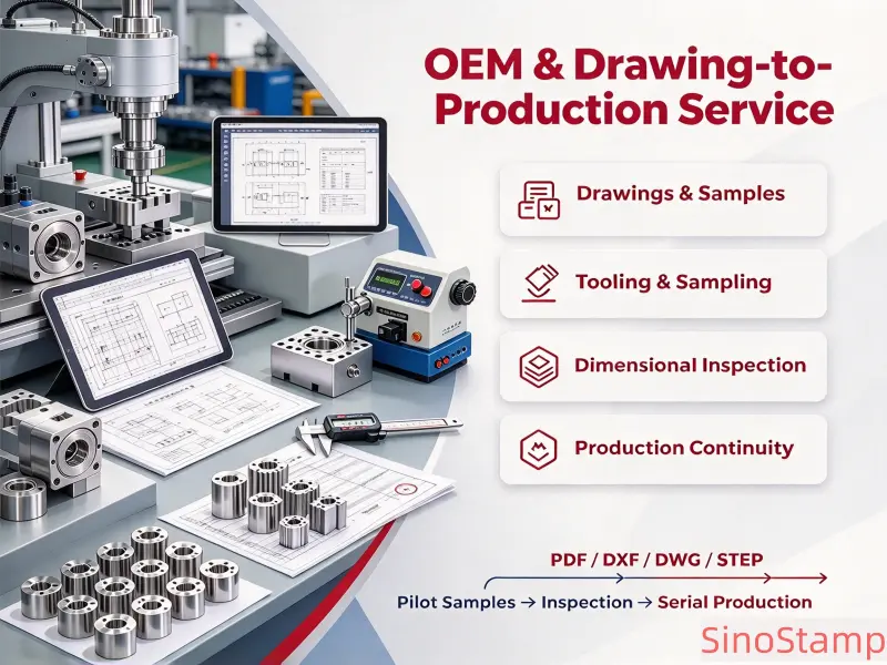
Engineering drawings provide the technical foundation for custom component manufacturing. They should identify material grade, thickness, dimensions, tolerances, surface finish, and critical features. Customers can provide PDF drawings, 2D CAD files, 3D models, and relevant product documentation for initial evaluation.
Prototype samples allow customers to evaluate dimensions, physical fit, assembly compatibility, and selected functional characteristics before regular production. Depending on the component, additional testing may be required to assess spring behavior, electrical contact performance, or shielding effectiveness at the assembly level. Testing requirements and acceptance criteria should be agreed during project development.
We understand that electronic product projects may begin with relatively small quantities during development and validation. Suitable small-batch manufacturing projects can be evaluated according to part complexity, tooling requirements, material availability, and production arrangements. For customers with ongoing demand, repeat orders can be coordinated based on approved drawings, established specifications, and agreed quality requirements.
Electronic metal stamping components are used across a wide range of products and industries. Their applications include electromagnetic shielding, circuit protection structures, electrical connections, battery interfaces, mechanical mounting, and internal equipment support. The exact component design depends on the electronic system, assembly configuration, operating environment, and performance requirements.
Wireless communication equipment may incorporate shielding covers, PCB shielding cans, brackets, and contact components. These parts support the physical structure of electronic assemblies and help manage electromagnetic interference around selected circuits. Component dimensions and contact arrangements should be coordinated with the PCB layout and enclosure design.
Consumer electronic products often require compact metal parts with consistent dimensions and suitable surface finishes. Examples include battery contacts, electronic spring contacts, shielding covers, and internal mounting brackets. These components may be manufactured in repeat quantities for electronic product assembly operations.
Computer and networking equipment can use metal shielding structures, internal brackets, contact components, and mounting parts. These products may require carefully controlled geometry to accommodate compact PCB assemblies and multiple internal components. Custom stamped parts can be designed according to the dimensions and installation conditions of the equipment.
Industrial control products may include stamped metal brackets, conductive contacts, shielding structures, and internal support components. Depending on the operating environment, material strength, corrosion resistance, dimensional stability, and assembly compatibility can be important selection criteria.
Choosing a manufacturing supplier for electronic components requires consideration of both technical and commercial factors. OEM customers need components that match their product drawings and can be manufactured consistently at the required quantity and quality level. SinoStamp focuses on custom electronic metal stamping projects and works with customers to evaluate manufacturing requirements before production.
Our electronic metal stamping product range includes EMI shielding covers, PCB shielding cans, electronic metal brackets, battery contact components, and electronic spring contacts. These products cover important functions in electronic assemblies, including shielding, electrical connection, positioning, and structural support.
We support non-standard components manufactured according to customer drawings, samples, and technical documentation. This allows customers to source parts designed for their own electronic assemblies rather than relying only on standard products. Material specifications, geometry, tolerances, and surface finishing can be evaluated according to project requirements.
Tooling selection should consider component geometry, material, production volume, and the expected product life cycle. We encourage customers to provide both technical drawings and estimated order quantities so that the manufacturing process can be evaluated more effectively. A suitable production arrangement can help balance tooling investment and repeat manufacturing efficiency.
International OEM projects require clear communication regarding technical specifications, samples, quotations, tooling, production schedules, inspection requirements, and shipping arrangements. We aim to maintain practical communication throughout the sourcing and manufacturing process so that customers can make informed purchasing decisions.
If your company is sourcing custom electronic metal stamping parts for a new product or an existing production program, SinoStamp welcomes your inquiry. We support projects involving EMI shielding covers, PCB shielding cans, electronic metal brackets, battery contact components, and electronic spring contacts. Customers can provide engineering drawings, 3D models, physical samples, or technical specifications for an initial manufacturing review.
To help us evaluate your project, please include the material grade, thickness, critical dimensions, surface finishing requirements, expected order quantity, and intended application whenever possible. If your project requires custom tooling, prototype samples, or special inspection arrangements, these details can also be included in the initial inquiry.
After reviewing the available information, the manufacturing requirements can be discussed, including material selection, tooling approach, production process, sample development, and quotation details. Our goal is to help electronic equipment manufacturers and component buyers establish a practical supply solution for their custom stamped metal components.
Contact SinoStamp to discuss your electronic metal stamping requirements and explore a suitable OEM or ODM manufacturing arrangement in China.
```