EMI Shielding Covers Manufacturer in China
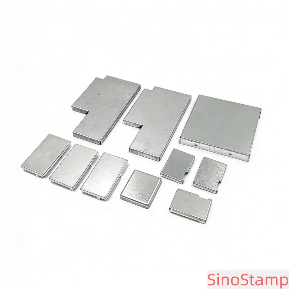
SinoStamp is a China-based manufacturer and supplier of custom EMI shielding covers for electronic component manufacturers, PCB assembly companies, communication equipment producers, and OEM electronics brands. We provide precision metal stamping solutions for shielding components used to reduce electromagnetic interference and help protect sensitive electronic circuits from unwanted electromagnetic coupling.
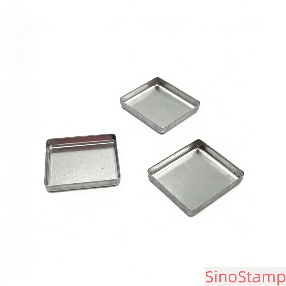
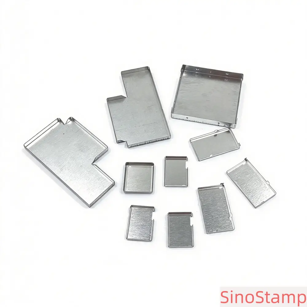
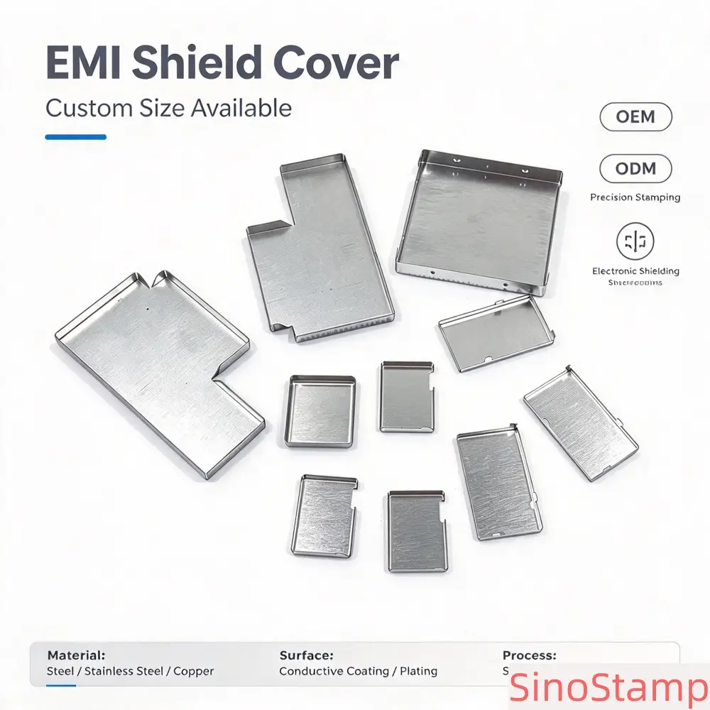
EMI shielding covers are widely used in printed circuit boards, WiFi modules, Bluetooth modules, wireless communication devices, consumer electronics, and other electronic assemblies. These components are typically manufactured from thin metal sheets and formed into customized covers, cans, or enclosures that fit specific circuit layouts and electronic components.
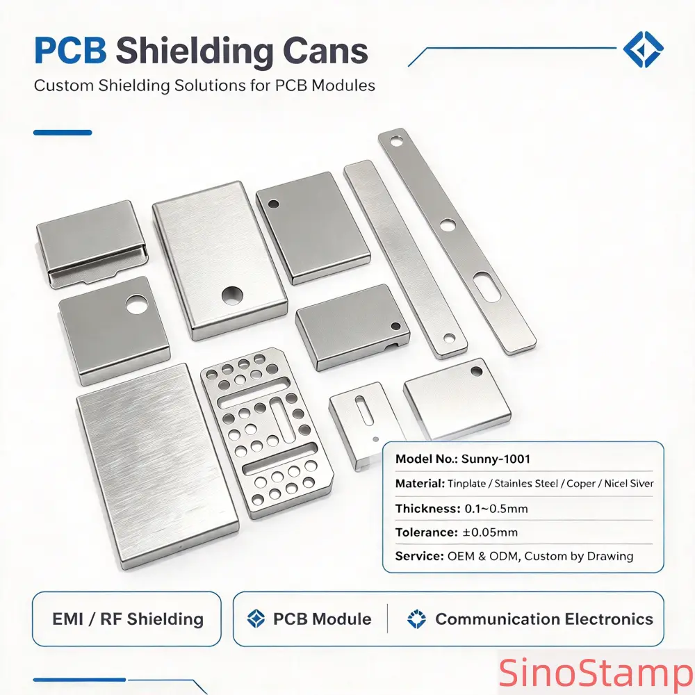
Our model Sunny-1001 is a customizable EMI shielding cover designed for OEM and ODM projects. Available materials include tinplate, stainless steel, copper, and nickel silver. Material thickness can range from 0.1 mm to 0.5 mm, depending on the design and application requirements. We support precision stamping, bending, forming, and customized surface finishing to meet different electronic assembly specifications.
Whether you need a simple shielding cover for a single electronic component or a more complex stamped shielding structure for a PCB assembly, SinoStamp can review your drawings, samples, and technical specifications to evaluate manufacturing feasibility and provide a suitable production solution.
Sunny-1001 EMI Shielding Covers Product Specifications
Sunny-1001 is a customizable metal shielding component manufactured according to customer drawings, dimensions, and application requirements. The following specifications provide a general overview of available options. Final specifications can be confirmed according to the approved engineering drawing and project requirements.
- Model No.: Sunny-1001
- Product Name: EMI Shielding Covers
- Material: Tinplate / Stainless Steel / Copper / Nickel Silver (Customizable)
- Thickness: 0.1mm ~ 0.5mm (Customizable)
- Surface Finish: Bright tin plating / Matte / Anti-tarnish treatment
- Processing: Precision stamping, bending, forming
- Function: EMI & RF shielding, designed to help suppress electromagnetic interference
- Custom Service: OEM & ODM, custom size, shape, and drawing-based production
- Application: PCB, WiFi module, Bluetooth module, communication electronics
- Tolerance: ±0.05mm for critical dimensions, subject to design and process feasibility
- Sample: Sample production and testing supported
- Packing: Anti-static bag + carton
Customers can specify the required material, thickness, dimensions, surface finish, and assembly method. For projects involving special shielding performance requirements, the target frequency range, shielding effectiveness, grounding structure, and test method should be discussed before sample production.
What Are EMI Shielding Covers?
EMI shielding covers are metal components used to enclose or partially cover sensitive electronic circuits and components. Their purpose is to reduce the effects of electromagnetic interference by providing a conductive barrier around selected areas of an electronic assembly. Depending on the design, these covers may be installed directly onto a PCB, attached to a shielding frame, or integrated into a larger electronic enclosure.
Electromagnetic interference can affect electronic devices in different ways. It may cause unwanted signals, communication instability, reduced circuit performance, or interference between nearby electronic components. As electronic products become smaller and more densely integrated, controlling electromagnetic interference becomes increasingly important for product designers and electronics manufacturers.
A properly designed metal shielding cover can help reduce electromagnetic coupling between sensitive circuits and external or neighboring sources of interference. Its effectiveness depends on several factors, including material conductivity, metal thickness, cover geometry, enclosure gaps, grounding connections, frequency range, and the overall PCB assembly design.
For this reason, selecting an EMI shielding cover should not be based on material choice alone. The complete shielding structure and its integration with the electronic assembly should be evaluated according to the intended operating conditions and applicable test requirements.
Custom EMI Shielding Covers for PCB Assemblies
PCB shielding covers are commonly used to separate sensitive electronic circuits from other components on a printed circuit board. They may be designed to cover a specific chip, RF circuit, wireless communication module, power section, or other area requiring electromagnetic interference control.
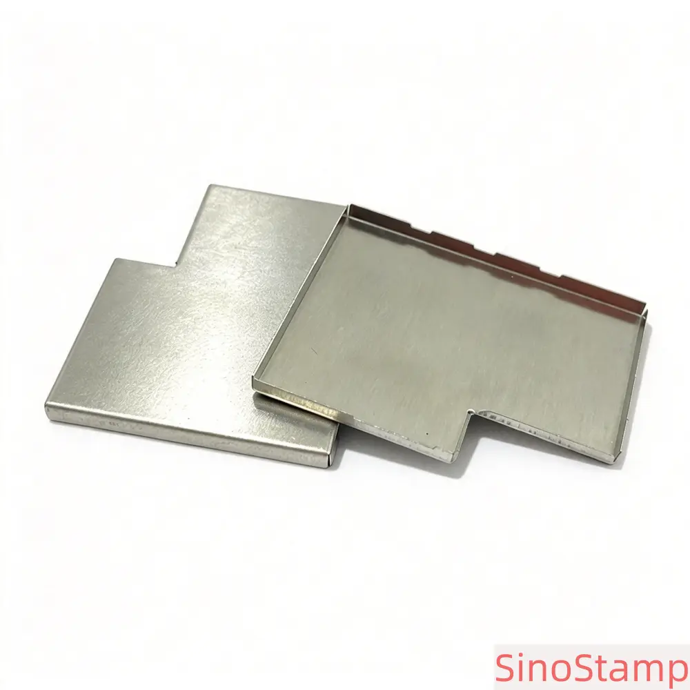
Depending on the application, a PCB shielding cover may be a simple one-piece metal cover or a more complex component with multiple walls, formed edges, mounting features, and grounding contact areas. Some designs use a separate shielding frame and removable cover, while others use a single stamped metal structure.
SinoStamp supports customized PCB shielding cover manufacturing based on customer drawings and samples. We can review the overall dimensions, wall height, corner geometry, mounting structure, material thickness, and other features that influence fit and production feasibility.
Common PCB shielding cover design requirements include:
- Custom length, width, and height according to PCB layout.
- Specific wall thickness and cover geometry.
- Precise mounting holes, slots, and positioning features.
- Formed edges and corners for assembly compatibility.
- Material selection based on shielding and mechanical requirements.
- Surface finishing suitable for the intended electronic application.
- Compatibility with shielding frames, soldering, or other mounting methods.
For customers developing new PCB products, supplying a complete mechanical drawing or 3D CAD model can help reduce design misunderstandings. If only a physical sample is available, we can review the sample and discuss the information required for a customized manufacturing proposal.
Materials for Custom EMI Shielding Covers
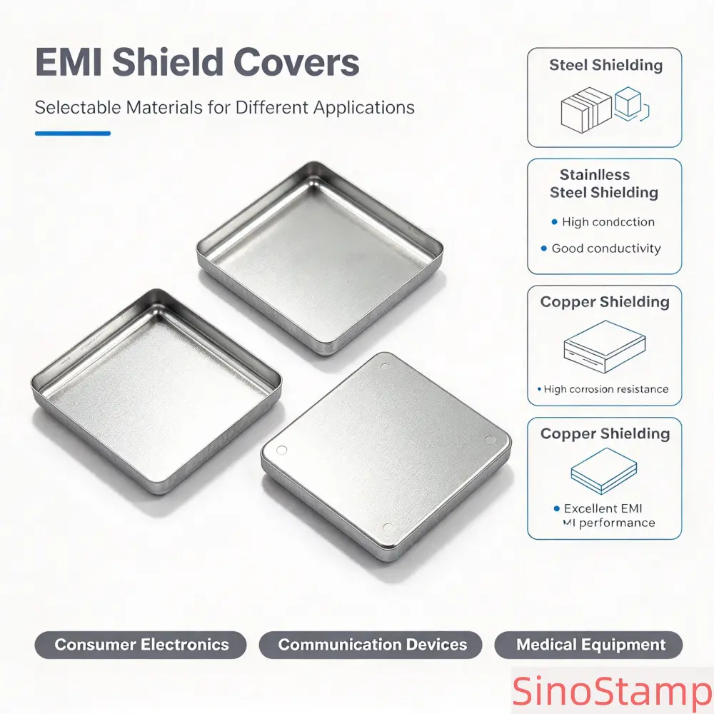
Material selection is one of the most important considerations in EMI shielding cover manufacturing. Different metals offer different combinations of electrical conductivity, magnetic properties, corrosion resistance, mechanical strength, formability, and cost. The best material depends on the shielding objective, operating frequency, component structure, and manufacturing requirements.
Tinplate EMI Shielding Covers
Tinplate is a steel sheet coated with a thin layer of tin. It combines the mechanical strength of steel with a tin-coated surface and is commonly considered for electronic shielding components. Its formability and surface characteristics make it suitable for various stamped shielding cover designs.
Tinplate can be used for customized shielding covers that require a balance between structural strength, manufacturability, and cost. It may be suitable for applications involving small metal enclosures, PCB shielding covers, and other electronic components.
When selecting tinplate, customers should confirm the base material specification, tin coating requirements, thickness, and surface condition. These details can affect forming performance, soldering compatibility, corrosion resistance, and the final appearance of the component.
Stainless Steel EMI Shielding Covers
Stainless steel offers good corrosion resistance and mechanical strength. It may be suitable for shielding cover designs where structural stability, durability, and resistance to environmental exposure are important.
Different stainless steel grades have different forming and magnetic characteristics. The selected grade should therefore be evaluated according to the part geometry and application. For thin stamped shielding components, material thickness and forming conditions should also be reviewed to avoid unnecessary deformation.
Stainless steel is not automatically the best choice for every EMI shielding application. Electrical conductivity and magnetic behavior differ from other available metals, so the material should be selected according to the actual shielding requirements and tested where necessary.
Copper EMI Shielding Covers
Copper is known for its high electrical conductivity and is widely used in electrical and electronic applications. It may be suitable for shielding cover designs where conductivity and specific material characteristics are important.
Copper is available in different grades and tempers, which can influence its mechanical properties and formability. For custom shielding covers, customers should specify the required copper grade, thickness, and temper where applicable.
Although copper offers high electrical conductivity, the shielding performance of a finished cover still depends on its complete geometry, grounding arrangement, assembly gaps, and operating frequency. The final design should be evaluated in the intended electronic assembly.
Nickel Silver EMI Shielding Covers
Nickel silver, also known as copper-nickel-zinc alloy, is used in selected electronic and precision metal component applications. It offers a combination of mechanical properties, appearance, and corrosion resistance that may be suitable for customized shielding cover designs.
Nickel silver is not a silver-containing precious metal. Its properties vary according to alloy composition and material grade. Customers should confirm the required alloy specification, thickness, and forming characteristics before production.
How to Select the Right Material
Choosing the appropriate material requires consideration of the actual application rather than simply comparing conductivity values. A suitable material should meet the required shielding objective while also providing acceptable formability, mechanical strength, surface quality, and production cost.
For OEM projects, we recommend confirming the following details during material selection:
- Required shielding frequency range.
- Target shielding effectiveness or attenuation in dB.
- Material grade and electrical or magnetic properties.
- Required thickness and dimensional tolerances.
- Forming complexity and mechanical strength.
- Corrosion resistance and operating environment.
- Soldering, grounding, and assembly requirements.
- Surface finishing and appearance specifications.
Material Thickness and Precision Stamping
Sunny-1001 EMI shielding covers can be manufactured using material thicknesses from 0.1 mm to 0.5 mm, subject to the selected material and component design. Thin metal sheets are commonly used for electronic shielding components because they allow compact structures and can be formed into customized shapes.
However, material thickness should be selected according to the component's mechanical and electrical requirements. A thinner sheet may help reduce weight and material consumption, while a thicker sheet may provide greater rigidity and structural stability. The correct choice also depends on the cover dimensions, wall height, forming geometry, and mounting method.
For thin stamped metal components, tooling accuracy and process control are important. Variations in material thickness, punching clearance, bending conditions, or die alignment may influence the final dimensions and appearance.
SinoStamp can review the customer's target thickness and component geometry to evaluate the feasibility of the proposed stamping process. Where critical dimensions are involved, the inspection plan should identify the specific features that require tighter control.
Precision Stamping, Bending, and Forming Processes
Custom EMI shielding covers are generally manufactured through a combination of metal stamping operations. The manufacturing process depends on the shape, dimensions, material, required production quantity, and assembly design.
Precision Blanking
Blanking creates the initial profile of the shielding cover from a metal sheet or strip. The blanking process determines the basic shape and establishes the material geometry for subsequent forming operations.
For small electronic shielding components, cutting accuracy and edge quality can influence the fit of the finished cover. Tooling design should consider material thickness, punching clearance, and the required dimensional tolerances.
Punching and Piercing
Punching is used to create openings, slots, mounting features, and other required details. Some shielding cover designs include locating holes, tabs, relief features, or other geometries that help the component fit into the PCB assembly.
Hole positions and feature dimensions should be controlled according to the engineering drawing. Where the cover must align with a separate shielding frame or PCB mounting points, these dimensions may be identified as critical inspection features.
Bending and Forming
Bending and forming operations transform flat metal blanks into three-dimensional shielding covers. Depending on the design, the process may create side walls, flanges, folded edges, corners, and other structural features.
Springback, material thickness, bend radius, and forming sequence can affect the final geometry. These factors should be considered during tooling development, particularly for small covers with narrow walls or multiple bends.
Progressive Die Stamping
Progressive die stamping may be suitable for shielding covers with stable demand and production quantities that justify dedicated tooling. Multiple operations are performed at different stations as the metal strip advances through the die.
This approach can support efficient repeat production when the component design and production volume are appropriate. Tooling cost, design complexity, and expected order quantities should be evaluated before selecting a progressive die solution.
Surface Finishing Options for EMI Shielding Covers
Surface finishing can influence corrosion resistance, appearance, electrical contact behavior, and compatibility with the customer's assembly process. The appropriate finish depends on the base material, intended application, environmental conditions, and technical requirements.
Bright Tin Plating
Bright tin plating provides a bright metallic surface and may be selected for electronic components requiring a tin-finished surface. Depending on the design, tin plating may also be considered where soldering compatibility or electrical contact requirements are relevant.
Customers should specify the required plating thickness, surface appearance, and applicable technical standards. Plating requirements should be confirmed before production because they may influence dimensions and assembly clearances.
Matte Surface Finish
A matte finish provides a non-glossy surface appearance and may be selected for specific product or assembly requirements. The final surface condition depends on the base material and finishing process. Customers should provide appearance references or approved samples when surface consistency is important.
Anti-Tarnish Treatment
Anti-tarnish treatment may be considered for selected metal surfaces where appearance stability and resistance to surface discoloration are important. The treatment should be compatible with the base material and the intended application.
For electronic shielding components, customers should also evaluate whether the selected surface treatment is compatible with grounding contacts, soldering, electrical connections, and other assembly processes.
EMI and RF Shielding Performance Considerations
The main function of an EMI shielding cover is to help reduce electromagnetic interference affecting sensitive electronic circuits. However, shielding effectiveness is not determined by the metal material alone. The final result depends on the complete shielding structure and how it is integrated into the electronic device.
Important factors include material conductivity, magnetic properties, thickness, enclosure geometry, opening size, seams, contact resistance, grounding arrangement, and the frequency range of interest. Even a highly conductive material may not provide the expected result if the cover has large gaps or poor electrical contact with the surrounding structure.
For RF applications, the design of the cover and its connection to the PCB or shielding frame can be particularly important. The customer should define the target frequency range and shielding performance requirements before selecting a material and manufacturing approach.
Shielding Effectiveness in dB
Shielding effectiveness is commonly expressed in decibels (dB). A higher measured value generally indicates greater attenuation under the specific test conditions. However, a shielding effectiveness value is meaningful only when the test method, frequency range, sample configuration, and measurement conditions are clearly identified.
SinoStamp can discuss material and sample testing requirements with customers who need to verify shielding performance. Where available, customers may provide an existing material test report or a target shielding specification to guide the project evaluation.
We recommend confirming the following information for performance-related projects:
- Target frequency range, such as the specific RF bands relevant to the product.
- Required shielding effectiveness in dB.
- Material type and thickness to be evaluated.
- Whether testing is required on flat material, a stamped cover, or a complete assembly.
- Test method and laboratory requirements.
- Grounding and mounting conditions used during testing.
- Required report language and documentation format.
Material Testing and Finished-Part Testing
Material testing and finished-part testing are not necessarily equivalent. A flat sheet material report provides information about the tested material under the laboratory's stated conditions. It does not automatically prove that a finished shielding cover or assembled electronic product will achieve the same shielding effectiveness.
Finished-part performance may be influenced by forming geometry, seams, gaps, mounting contacts, grounding, and the surrounding PCB structure. For applications with strict EMI requirements, finished-cover or assembly-level testing may therefore be necessary.
For this reason, the testing scope should be agreed before sample production. Customers can specify whether they need a material report, a stamped-part test, or a test of the complete shielding assembly. The selected test facility and method should be confirmed according to the project's technical requirements.
Dimensional Tolerances and Quality Control
Precision is essential for EMI shielding covers because these components often need to fit within compact electronic assemblies. Incorrect dimensions can create assembly difficulties, gaps, poor contact, or interference with neighboring components.
For Sunny-1001, a tolerance of ±0.05 mm can be considered for critical dimensions, subject to the component geometry, material thickness, tooling design, and production feasibility. The final tolerance requirements should be clearly marked on the approved engineering drawing.
Critical Dimensions
Common critical dimensions may include overall length and width, cover height, wall position, mounting features, opening dimensions, and the distance between locating points. Customers should identify which dimensions are functionally important so that inspection resources can be focused appropriately.
First Article Inspection
Initial samples can be inspected against the approved drawing before regular production. Depending on the part, inspection may include dimensional measurements, visual checks, forming geometry, surface condition, and fit verification with the customer's reference assembly.
Visual and Surface Inspection
Visual inspection may be used to identify dents, scratches, cracks, deformation, plating defects, and other surface issues. Edge condition and burr direction should also be considered where they affect assembly or handling.
Production Consistency
For repeat orders, stable tooling conditions, consistent material specifications, and controlled production processes are important. Customers may define inspection frequency, batch identification, and documentation requirements according to their quality management system.
OEM and ODM Custom EMI Shielding Cover Manufacturing
SinoStamp supports OEM and ODM projects for customers that require customized shielding components. We can work from complete engineering drawings, 3D CAD files, reference samples, or preliminary design information.
OEM Production Based on Drawings
For customers with an established design, we can manufacture shielding covers according to approved drawings and technical specifications. These documents should identify the material, thickness, dimensions, tolerances, surface finish, and other relevant requirements.
ODM Design and Manufacturing Coordination
For customers developing a new shielding structure, we can review the proposed geometry and discuss practical manufacturing considerations. This may include material selection, forming feasibility, mounting features, and production tooling options.
Any engineering changes that affect the intended shielding function or product interface should be reviewed and approved by the customer before implementation.
Custom Sizes and Shapes
Shielding covers are often designed to match a specific PCB layout or electronic module. We support customized length, width, height, wall geometry, corner design, mounting features, and other dimensions according to customer requirements.
Custom Tooling
Depending on the design and order quantity, dedicated stamping tooling may be required. Tooling development should consider part complexity, dimensional tolerances, production volume, and expected repeat orders. Customers should confirm tooling cost, ownership, maintenance, and storage arrangements as part of the project agreement.
Applications of EMI Shielding Covers
Custom EMI shielding covers are used in many electronic products where electromagnetic interference needs to be controlled. The specific cover design depends on the electronic circuit, available installation space, operating frequency, and assembly structure.
PCB and Electronic Circuit Boards
PCB shielding covers can be installed over selected circuit areas to reduce unwanted electromagnetic coupling. They may be used around sensitive chips, RF circuits, communication sections, and other components requiring localized shielding.
WiFi Modules
WiFi modules are commonly integrated into routers, gateways, smart home devices, industrial communication equipment, and consumer electronics. Shielding components may be included in the module design to help manage interference between different circuit sections.
Bluetooth Modules
Bluetooth modules are used in wireless accessories, smart devices, audio products, and connected electronic equipment. Custom shielding covers may be designed to fit the module's PCB dimensions and mechanical structure.
Communication Electronics
Communication equipment may contain multiple RF circuits and electronic components operating within compact spaces. Shielding covers can be used to separate selected circuit sections and support the overall electromagnetic compatibility design.
Consumer and Industrial Electronics
Other possible applications include smart home devices, wireless controllers, electronic modules, IoT products, industrial control boards, and compact communication equipment. The suitability of a specific shielding cover should be evaluated against the product's design and testing requirements.
Packaging for Custom EMI Shielding Covers
Packaging is important for small precision metal components because parts may be vulnerable to scratches, deformation, contamination, or surface damage during transportation and handling.
Sunny-1001 can be packed using anti-static bags and cartons according to the agreed packing requirements. For electronic manufacturing customers, packaging quantity, labeling, batch identification, and handling instructions can be customized where necessary.
Depending on the component geometry and surface finish, additional protective packaging may be considered to prevent parts from rubbing against each other. Customers should confirm whether individual separation, compartment packaging, or other protective methods are required.
Sample Production and Testing Support
Sample production allows OEM customers to evaluate component dimensions, fit, surface quality, and manufacturing feasibility before moving into regular production. For EMI shielding covers, sample evaluation may also include assembly checks and shielding performance testing when required.
SinoStamp supports sample testing discussions for Sunny-1001 projects. The sample quantity, tooling approach, material availability, and production lead time should be confirmed according to the component design.
Before requesting samples, customers are encouraged to provide:
- Engineering drawings or 3D CAD files.
- Preferred material and thickness.
- Required surface finish.
- Critical dimensions and tolerances.
- PCB or assembly interface information.
- Target shielding frequency range and performance requirements, if applicable.
- Sample quantity and testing requirements.
Once the sample specifications are confirmed, customers can evaluate whether additional testing is required. For projects with strict shielding targets, the test method and laboratory should be agreed before the samples are submitted for evaluation.
Why Choose SinoStamp for EMI Shielding Covers?
Choosing an EMI shielding cover supplier involves evaluating material options, precision manufacturing capability, dimensional control, surface finishing, and the ability to support customized electronic components. SinoStamp focuses on drawing-based OEM and ODM manufacturing for customers seeking custom stamped metal parts from China.
Multiple Material Options
We support tinplate, stainless steel, copper, and nickel silver options, subject to the requirements of the project. This allows customers to evaluate different material characteristics according to their shielding objectives and production needs.
Customized Thickness and Geometry
Material thickness from 0.1 mm to 0.5 mm can be considered for Sunny-1001, with custom dimensions and shapes based on customer drawings. Final feasibility depends on material selection and component geometry.
Precision Stamping and Forming
Our manufacturing focus includes precision stamping, bending, and forming for custom shielding components. Process planning should be based on the required dimensions, material characteristics, and production volume.
OEM and ODM Support
We work with customers that have established drawings as well as those that need manufacturing coordination during product development. Custom tooling and production options can be evaluated according to project requirements.
Sample Evaluation
Sample production provides an opportunity to check component fit, dimensions, appearance, and other specified characteristics before regular production. Shielding performance testing can be discussed separately according to the agreed test scope.
B2B Project Coordination
We understand the importance of clear technical communication for electronic component sourcing. Customers can share drawings, specifications, samples, and estimated order quantities to support a structured project review and quotation process.
Information Required for an EMI Shielding Covers Quotation
To prepare an accurate quotation for custom EMI shielding covers, please provide the following information where available:
- Product drawing or 3D CAD file.
- Required material: tinplate, stainless steel, copper, or nickel silver.
- Material thickness and applicable material grade.
- Overall dimensions and critical tolerances.
- Surface finishing requirements.
- Mounting and grounding structure.
- PCB or electronic module application.
- Required shielding frequency range and target dB value, if specified.
- Sample quantity and expected mass production quantity.
- Required testing method or laboratory, if applicable.
- Destination country and packaging requirements.
If you do not yet have a complete engineering drawing, you can provide a reference sample or preliminary design information for an initial review. The final manufacturing specifications should be confirmed before tooling and production begin.
Custom EMI Shielding Covers from China for OEM Electronics Manufacturers
SinoStamp provides customized EMI shielding cover manufacturing solutions for electronic component manufacturers, PCB assembly companies, communication equipment producers, and OEM electronics brands. Our Sunny-1001 model supports a range of material options, customizable thicknesses, precision stamping, bending, forming, and surface finishing.
We understand that an EMI shielding cover must do more than match the external dimensions of a PCB. Its material, geometry, mounting structure, grounding contact, and assembly conditions may all influence the final shielding performance. For this reason, we encourage customers to define their technical requirements clearly and evaluate samples under the intended application conditions.
Whether you need a small initial sample order or a long-term supply program, SinoStamp can review your drawings and discuss a suitable manufacturing approach. Contact us with your technical specifications to start your custom EMI shielding cover project.
```