PCB Shielding Cans Manufacturer in China
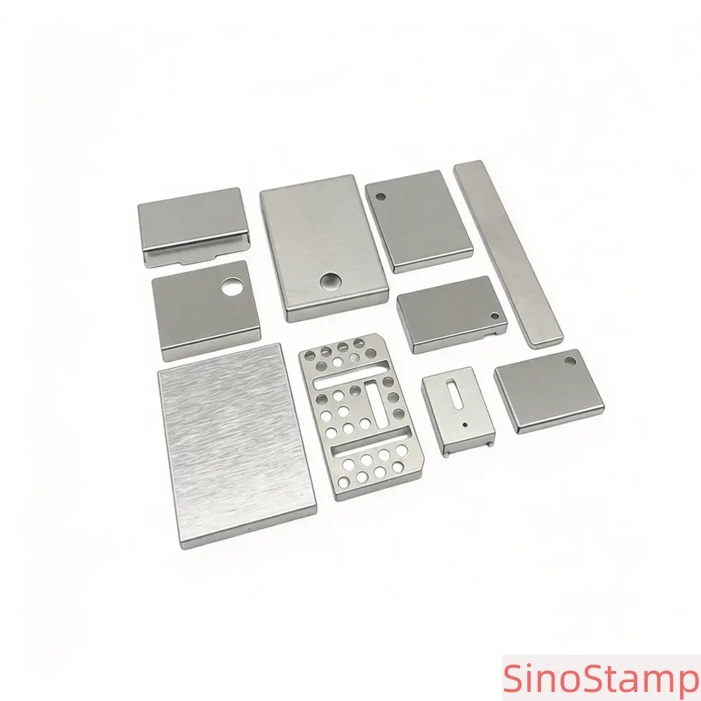
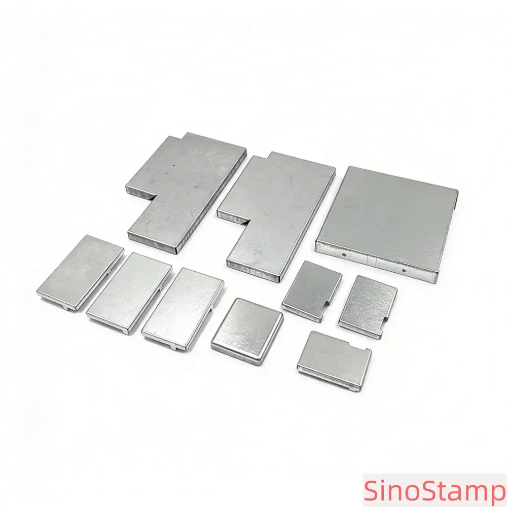
SinoStamp is a China-based manufacturer and supplier of custom PCB shielding cans for electronic component manufacturers, PCB assembly companies, wireless communication equipment producers, and OEM electronics brands. We provide customized metal stamping solutions for shielding components used to help reduce electromagnetic interference (EMI) and radio frequency interference (RFI) in electronic circuits.
PCB shielding cans are widely used in wireless communication modules, WiFi devices, Bluetooth products, RF communication systems, industrial control boards, consumer electronics, and other electronic assemblies. They are designed to cover selected areas of a printed circuit board, creating a conductive shielding structure around sensitive components and circuit sections.
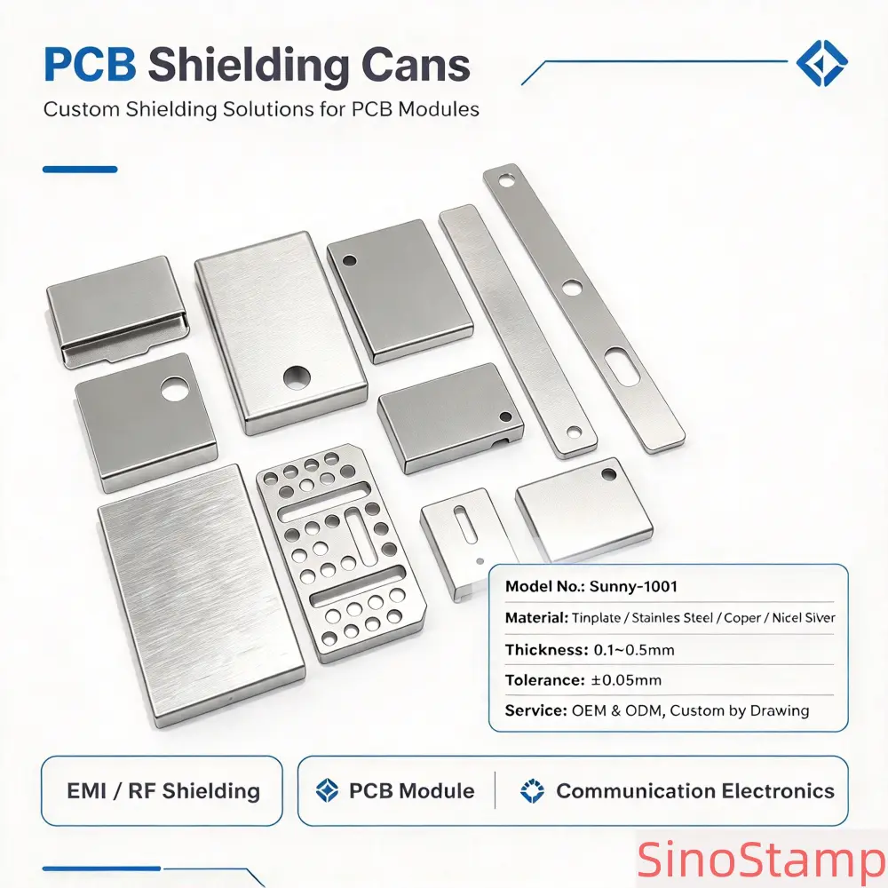
Our model Sunny-1002 is a customizable PCB shielding can manufactured according to customer drawings, samples, and technical specifications. Available material options include tinplate, stainless steel, copper, and nickel silver. Material thickness ranges from 0.1 mm to 0.6 mm, depending on the design and application requirements. Manufacturing processes can include deep drawing, precision stamping, bending, and forming.
We support OEM and ODM projects that require customized dimensions, shapes, cutouts, mounting features, and surface finishes. Whether your project involves a simple PCB shielding can or a more complex formed metal enclosure, our team can review your design and discuss suitable manufacturing processes, materials, tooling, and sample requirements.
Sunny-1002 PCB Shielding Cans Product Specifications
Sunny-1002 is a customizable metal shielding component designed for PCB and electronic module applications. The following specifications provide an overview of available manufacturing options. Final specifications should be confirmed according to the customer's approved engineering drawing and project requirements.
- Model No.: Sunny-1002
- Product Name: PCB Shielding Cans
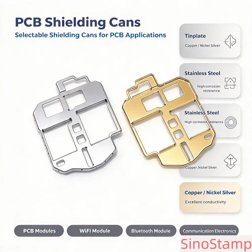
- Material: Tinplate / Stainless Steel / Copper / Nickel Silver (Customizable)
- Thickness: 0.1mm ~ 0.6mm (Customizable)
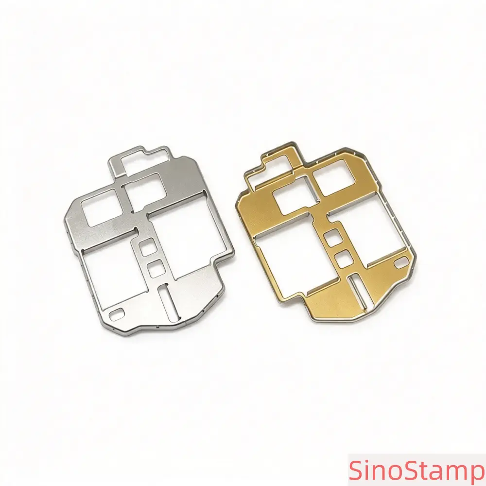
- Surface Finish: Bright tin plating / Matte / Anti-tarnish treatment / Gold plating
- Processing: Deep drawing, precision stamping, bending, forming
- Function: EMI & RF shielding, designed to help suppress electromagnetic interference for PCB assemblies
- Custom Service: OEM & ODM, custom size, shape, and cutouts based on customer drawings
- Application: PCB boards, WiFi modules, Bluetooth modules, RF communication modules
- Tolerance: ±0.05mm for critical dimensions, subject to design and process feasibility
- Certification: RoHS documentation and ISO 9001 quality management information available subject to applicable scope and verification; CE applicability depends on the finished product and relevant regulations
- Sample: Sample production and testing supported
- Packing: Anti-static bag + export carton
Customers can specify material grade, sheet thickness, overall dimensions, cutout locations, forming geometry, surface treatment, and assembly requirements. For projects with defined shielding targets, the required frequency range, shielding effectiveness in dB, grounding arrangement, and test method should be discussed before sample production.
What Are PCB Shielding Cans?
PCB shielding cans are metal enclosures or covers installed over selected areas of a printed circuit board to help control electromagnetic interference. They are commonly used to isolate sensitive electronic circuits from surrounding components and reduce unwanted electromagnetic coupling within compact electronic devices.
Modern electronic products often contain multiple circuits operating in close proximity. Wireless communication sections, processors, power circuits, RF components, and signal-processing modules may generate or receive electromagnetic energy. Without appropriate electromagnetic compatibility design, interference between these circuits can affect device performance, signal quality, or communication stability.
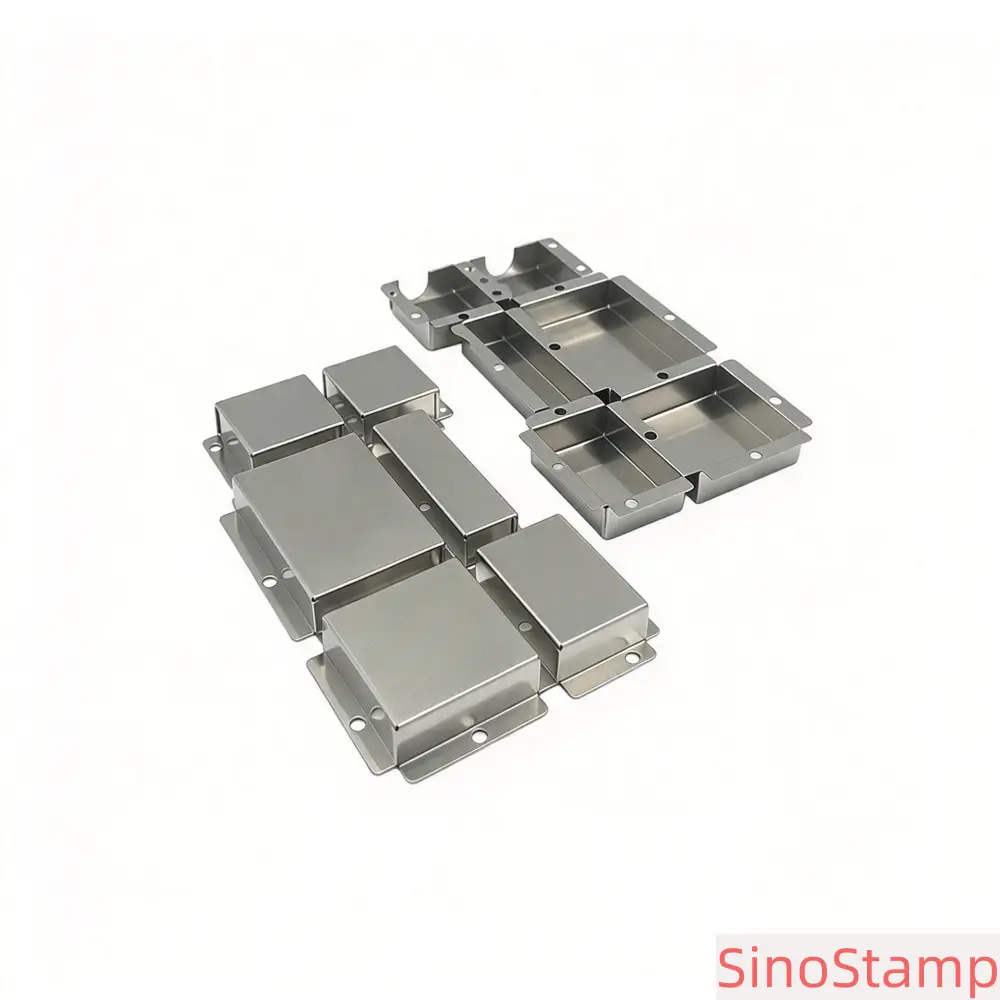
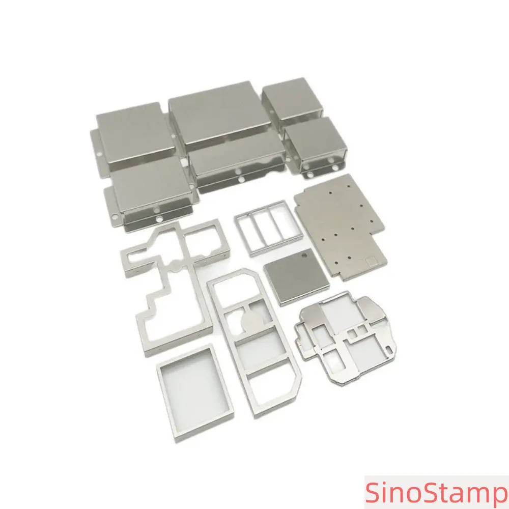
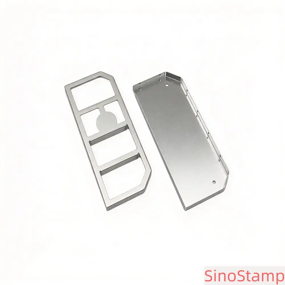
A PCB shielding can provides a conductive physical barrier around selected components. Depending on the design, it may be installed directly onto a PCB, attached to a separate shielding frame, or integrated into a larger electronic enclosure. Some shielding cans are manufactured as one-piece components, while others use a separate frame and removable cover.
The structure and installation method depend on the electronic module, PCB layout, available space, component height, grounding design, and required shielding performance. For this reason, PCB shielding cans are usually customized rather than selected solely from standard dimensions.
For OEM electronics manufacturers, a suitable shielding can should satisfy several requirements at the same time: accurate fit, appropriate material properties, reliable assembly, suitable surface finish, and performance consistent with the intended electromagnetic compatibility design.
Custom PCB Shielding Cans for Electronic Manufacturers
PCB shielding cans are often designed around a specific circuit layout. Their dimensions, wall height, cutouts, mounting points, and forming features must match the PCB and the components being protected. Even small dimensional differences can influence assembly clearance or the contact between the shielding structure and its mounting frame.
SinoStamp supports drawing-based PCB shielding can manufacturing for customers with established product designs and technical documentation. We can review the proposed geometry and manufacturing requirements before production to identify relevant tooling and process considerations.
Common customization options include:
- Custom length, width, and height based on PCB dimensions.
- Different wall heights to accommodate electronic components.
- Customized cutouts for connectors, cables, and other interfaces.
- Formed corners, flanges, tabs, and mounting features.
- Custom openings and relief features based on circuit layout.
- Material and thickness selection according to application requirements.
- Surface finishes for appearance, corrosion resistance, or assembly compatibility.
- One-piece or multi-component shielding structures, subject to design feasibility.
Customers can provide 2D drawings, 3D CAD files, physical samples, or preliminary design information. A complete drawing with dimensions and tolerances is preferred for quotation and manufacturing evaluation. If a physical sample is supplied, its critical features and interface requirements should also be identified.
Materials for Custom PCB Shielding Cans
Material selection has an important influence on shielding performance, mechanical strength, forming behavior, corrosion resistance, and manufacturing cost. Different metals offer different combinations of electrical conductivity, magnetic properties, and workability. The appropriate material depends on the target frequency range, shielding structure, assembly design, and operating environment.
Tinplate PCB Shielding Cans
Tinplate is a steel sheet coated with a thin layer of tin. It combines the structural strength of steel with a tin-coated surface and is commonly considered for electronic metal components. Its formability makes it suitable for various stamped shielding can designs.
Tinplate may be used for PCB shielding cans that require a balance between mechanical stability, manufacturing feasibility, and cost. It can be processed through cutting, punching, stamping, and forming operations to produce customized metal covers and enclosures.
When specifying tinplate, customers should confirm the base steel grade, tin coating requirements, sheet thickness, and surface condition. These factors can influence forming performance, soldering compatibility, corrosion resistance, and the final appearance.
Stainless Steel PCB Shielding Cans
Stainless steel offers corrosion resistance and mechanical strength. It may be suitable for shielding structures where durability, structural stability, or resistance to environmental exposure is important.
Different stainless steel grades have different forming characteristics, strength levels, and magnetic properties. The selected grade should be evaluated according to the required geometry and application. For thin-walled shielding cans, forming conditions and material springback should also be considered.
Stainless steel is not automatically the best material for every shielding application. Electrical conductivity and magnetic behavior vary from those of copper and other metals. Customers should select the grade based on the actual engineering requirements and validate the completed structure where necessary.
Copper PCB Shielding Cans
Copper is known for its high electrical conductivity and is widely used in electrical and electronic applications. It may be suitable for PCB shielding cans where conductivity is an important material consideration.
Different copper grades and tempers have different mechanical properties and forming characteristics. For custom deep-drawn or stamped shielding components, the selected copper specification should be reviewed together with the geometry, material thickness, and forming requirements.
Although copper offers high electrical conductivity, finished shielding performance also depends on enclosure design, contact resistance, grounding, seams, and frequency. A copper shielding can should therefore be evaluated as part of the intended electronic assembly.
Nickel Silver PCB Shielding Cans
Nickel silver is a copper-nickel-zinc alloy used in selected precision metal and electronic component applications. It offers a combination of mechanical properties, surface appearance, and corrosion resistance that may be suitable for certain shielding can designs.
Nickel silver does not contain silver as a precious-metal coating. Its characteristics depend on the specific alloy composition and material grade. Customers should identify the required grade and thickness when requesting a quotation or sample.
Material Selection for Different PCB Applications
There is no single material that is suitable for every PCB shielding can. A high-conductivity material may be desirable for some designs, while another application may prioritize mechanical stiffness, corrosion resistance, forming performance, or cost efficiency.
Before confirming a material, OEM customers should consider:
- The operating frequency range of the electronic circuit.
- The target shielding effectiveness and applicable test conditions.
- Electrical conductivity and magnetic characteristics.
- Required material thickness and mechanical strength.
- Deep drawing and bending requirements.
- Corrosion exposure and operating environment.
- Grounding, soldering, and electrical contact requirements.
- Surface finishing and compatibility with PCB assembly.
Deep Drawing and Precision Stamping for PCB Shielding Cans
Sunny-1002 supports manufacturing processes including deep drawing, precision stamping, bending, and forming. The suitable process depends on the shielding can's depth, geometry, wall structure, corner radius, material characteristics, and production quantity.
Deep Drawing
Deep drawing is a metal forming process used to transform a flat sheet metal blank into a three-dimensional shape through a punch and die. It is suitable for certain shielding can designs that require deeper walls or a formed enclosure structure.
The deep drawing process can reduce the need for multiple separate parts in suitable designs. However, the feasibility of deep drawing depends on material ductility, thickness, draw depth, corner radius, blank dimensions, and forming conditions.
For electronic shielding cans, dimensional consistency and wall geometry are important. The tooling design should consider material flow, possible thinning, wrinkling, cracking, and dimensional variation. These factors become particularly important for small components with relatively thin walls.
Precision Stamping
Precision stamping is used to produce accurate profiles, mounting features, cutouts, and other details. It may involve blanking, punching, piercing, and other operations performed using customized dies.
For PCB shielding cans, precision stamping can create locating features, openings, tabs, and mounting details required by the electronic assembly. Tooling accuracy and appropriate punching clearance help maintain dimensional consistency and edge quality.
Bending and Forming
Bending and forming operations create the required walls, flanges, corners, and other three-dimensional features. They are commonly used for shielding cans that are manufactured from folded sheet metal or require multiple formed sections.
Material thickness, bend radius, springback, forming direction, and the sequence of operations can influence the final dimensions. These factors should be evaluated during process planning to achieve the required shape and assembly fit.
Multi-Stage Forming
Some PCB shielding cans require more than one forming operation to achieve the final geometry. Multi-stage forming may be considered when the part includes deeper walls, complex corners, multiple cutouts, or other features that cannot be produced reliably in a single operation.
The appropriate process should be selected after reviewing the engineering drawing and expected order volume. For new projects, prototype evaluation can help identify potential forming and assembly issues before regular production begins.
Customized Cutouts and Structural Design
One of the main requirements in PCB shielding can manufacturing is customization of the enclosure geometry. Electronic modules often contain connectors, cables, antenna interfaces, mounting points, and components that require specific clearance. The shielding can must accommodate these features without interfering with the intended assembly.
Connector and Cable Cutouts
Some shielding cans require openings for connectors, cable routing, or external interfaces. The location and dimensions of these cutouts should be based on the PCB layout and mechanical assembly requirements.
Component Clearance Openings
PCB assemblies may contain components with different heights or special installation requirements. A shielding can may need localized openings or customized wall geometry to provide the required clearance. The design should also consider whether these openings affect the intended shielding structure.
Mounting Tabs and Positioning Features
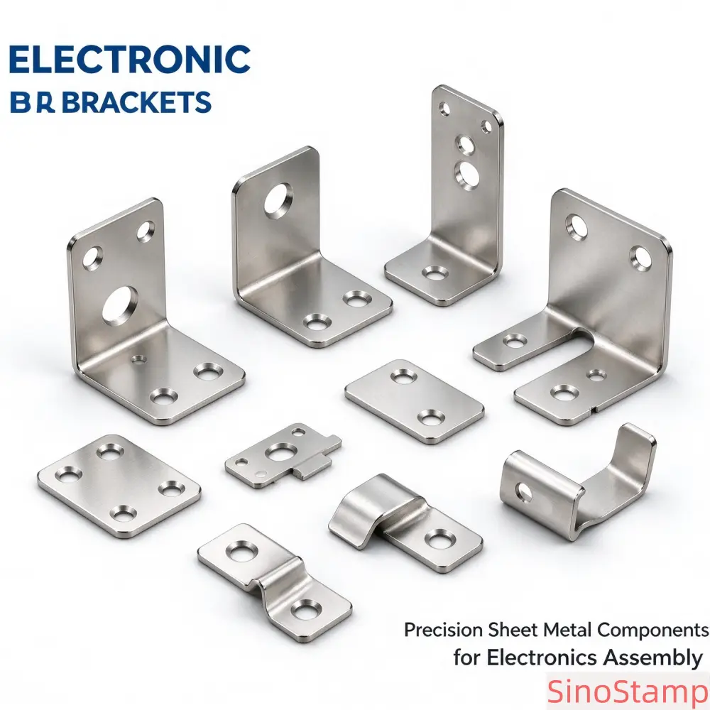
Mounting tabs, locating features, and formed edges can help position the shielding can during assembly. Their dimensions and locations should be coordinated with the PCB or shielding frame design.
Corner and Wall Geometry
Corner radius, wall height, flange width, and overall enclosure geometry influence both manufacturability and assembly compatibility. For deep-drawn components, corner design and material flow require particular attention during tooling development.
Customers are encouraged to provide the PCB outline and relevant component height information where possible. This helps the manufacturer understand the mechanical interfaces and evaluate the shielding can's design more accurately.
Surface Finishing Options for PCB Shielding Cans
Surface finishing can influence appearance, corrosion resistance, electrical contact behavior, solderability, and compatibility with the customer's assembly process. Sunny-1002 supports several surface finish options according to the selected base material and project specifications.
Bright Tin Plating
Bright tin plating provides a bright metallic surface and may be selected for electronic components where tin finishing is required. Depending on the design and assembly process, tin plating may also be considered for solderability or electrical contact requirements.
Customers should specify the required plating thickness, surface appearance, and relevant technical standards. Plating requirements should be reviewed together with dimensional tolerances and assembly clearances.
Matte Finish
A matte surface finish provides a non-glossy appearance and may be selected for specific component or product requirements. The final appearance depends on the base metal and finishing process. Approved samples or surface references can help establish the required visual standard.
Anti-Tarnish Treatment
Anti-tarnish treatment may be used for selected metal surfaces to help reduce discoloration during storage and handling. The treatment should be compatible with the base material and the intended electronic application.
Gold Plating
Gold plating may be specified for certain electronic applications where particular surface contact or corrosion-resistance characteristics are required. Its suitability depends on the actual electrical interface, required coating thickness, substrate, and cost target.
Gold plating is not automatically necessary for every PCB shielding can. Customers should clarify whether the finish is required for electrical contact, soldering, corrosion resistance, or another specific purpose. The plating specification should identify the required thickness and applicable acceptance criteria.
EMI and RF Shielding Performance for PCB Assemblies
The primary function of a PCB shielding can is to help reduce electromagnetic interference affecting sensitive electronic circuits. It provides a conductive enclosure around selected components or circuit sections. However, the final shielding effectiveness depends on the complete shielding structure rather than the metal material alone.
Important factors include material conductivity, magnetic properties, thickness, enclosure geometry, opening size, seams, contact resistance, grounding arrangement, and the frequency range of interest. The PCB layout and the way the shielding can is installed can also influence the result.
Shielding Effectiveness in Decibels
Shielding effectiveness is commonly expressed in decibels (dB). A higher measured value generally indicates greater attenuation under the specified test conditions. However, a shielding value is meaningful only when the frequency range, test method, sample configuration, and measurement conditions are clearly identified.
For OEM projects, customers should provide their target shielding effectiveness and operating frequency range wherever possible. This information helps guide material selection and shielding structure discussions.
Grounding and Electrical Contact
The electrical connection between the shielding can and the PCB or shielding frame is an important design consideration. Poor contact, gaps, or inconsistent grounding may reduce the effectiveness of the complete shielding structure.
Mounting features, contact surfaces, soldering areas, and the surrounding PCB layout should therefore be considered during the design stage. For designs with strict EMC requirements, assembly-level validation may be necessary.
Material Testing and Finished-Part Testing
A material shielding report and a finished PCB shielding can test report do not provide exactly the same information. A material report describes the performance of the tested material under the laboratory's stated conditions. It does not automatically demonstrate the performance of a finished, formed shielding can installed on a PCB.
Finished-part performance may be affected by the enclosure geometry, forming operations, seams, openings, grounding, mounting contacts, and PCB assembly. Where performance requirements are strict, customers may need to test the finished component or complete electronic assembly.
Before arranging testing, customers should confirm whether the required evaluation is for flat material, a stamped shielding can, or the assembled PCB. The test method, frequency range, laboratory, and report requirements should be agreed in advance.
Dimensional Tolerances and Precision Inspection
PCB shielding cans are frequently used in compact electronic products where available installation space is limited. Accurate dimensions are therefore important for ensuring proper fit and avoiding interference with neighboring components.
For Sunny-1002, a tolerance of ±0.05 mm can be considered for critical dimensions, subject to part geometry, material thickness, tooling design, and process feasibility. The final tolerances should be identified on the approved engineering drawing.
Critical Dimensions
Typical critical dimensions may include overall length and width, enclosure height, wall position, cutout dimensions, mounting features, and the distance between locating points. For deep-drawn components, additional attention may be required for corner geometry and wall consistency.
First Article Inspection
First article inspection helps verify that the initial samples meet the agreed drawing requirements. Depending on the design, inspection may include overall dimensions, wall height, opening positions, forming geometry, material thickness, and surface condition.
Visual and Surface Inspection
Visual inspection can identify scratches, dents, cracks, deformation, plating defects, and other visible issues. Edge quality and burr direction should also be checked where they affect assembly, handling, or product safety.
Repeat Production Control
For recurring orders, stable tooling conditions, consistent material specifications, and controlled production processes are important. Customers may define inspection frequency, batch identification, and documentation requirements according to their internal quality standards.
Quality Management and Compliance Documentation
Electronic component manufacturers often require suppliers to provide quality-related documentation as part of their purchasing and supplier approval processes. The specific documents depend on the customer's industry, product requirements, and applicable regulations.
RoHS Requirements
RoHS requirements restrict certain hazardous substances in electrical and electronic equipment within the applicable regulatory framework. Customers may request material declarations, supplier documentation, or test reports to support their compliance assessment.
For Sunny-1002 projects, RoHS-related documentation should be confirmed according to the selected material, surface treatment, and actual product specification. A material declaration or report should not be assumed to cover every possible material and finishing combination.
ISO 9001 Quality Management
ISO 9001 is a quality management system standard rather than a product performance certification. Customers may request information about the manufacturing supplier's quality management system and applicable certification scope as part of supplier evaluation.
Where ISO 9001 documentation is required, its validity, issuing body, certificate holder, and scope should be verified before being presented as evidence of certification.
CE Marking Considerations
CE marking is relevant to products covered by applicable European Union harmonisation legislation. A standalone PCB shielding can is not automatically required to carry CE marking simply because it is used in electronic equipment.
Whether CE requirements apply depends on the finished product, its intended function, and the relevant legislation. Customers should evaluate CE obligations at the finished equipment level where applicable and confirm the appropriate compliance responsibilities.
OEM and ODM PCB Shielding Can Manufacturing
SinoStamp supports OEM and ODM manufacturing projects for customers seeking customized PCB shielding cans. We can work with established engineering drawings or review preliminary designs to discuss manufacturing feasibility and production options.
OEM Production Based on Customer Drawings
For customers with completed product designs, we can manufacture shielding cans according to approved drawings and technical specifications. The documentation should include material, thickness, dimensions, tolerances, cutouts, forming details, surface finish, and other relevant requirements.
ODM Design and Manufacturing Coordination
For customers developing new electronic modules, we can discuss the practical manufacturing aspects of the proposed shielding structure. This may include material selection, deep drawing feasibility, forming sequence, wall geometry, mounting features, and surface finishing options.
Any engineering changes that may affect the intended shielding function or PCB interface should be reviewed and approved by the customer before implementation.
Custom Tooling Development
Custom PCB shielding cans may require dedicated stamping or deep drawing dies. Tooling design should consider part geometry, material thickness, forming depth, critical dimensions, and expected production quantities.
For customers planning long-term orders, tooling investment can be evaluated in relation to expected annual demand and production efficiency. Tooling ownership, maintenance responsibilities, storage arrangements, and usage rights should be agreed as part of the project terms.
Prototype and Sample Production
Sample production allows customers to evaluate dimensions, appearance, assembly fit, and manufacturing feasibility before regular production. The appropriate sample method depends on design complexity, tooling requirements, material availability, and requested quantity.
For projects with specific EMI performance requirements, sample testing can be discussed separately. The test scope should identify whether the evaluation applies to the material, finished shielding can, or complete PCB assembly.
Applications of PCB Shielding Cans
PCB shielding cans are used across different electronic industries where electromagnetic interference control is an important part of product design. The required shielding structure depends on the electronic circuit, operating frequency, mechanical layout, and assembly method.
WiFi Modules and Wireless Networking Equipment
WiFi modules are integrated into routers, gateways, smart home products, wireless controllers, industrial communication devices, and other connected electronics. Customized PCB shielding cans may be used around selected circuit sections to help manage electromagnetic interference within the module.
Bluetooth Modules
Bluetooth modules are widely used in wireless accessories, smart devices, audio products, and connected household equipment. Their compact circuit layouts may require customized shielding components that fit within limited installation spaces.
RF Communication Modules
RF communication modules are used in wireless transmitters, receivers, communication equipment, remote-control systems, and industrial devices. Shielding cans may be designed to enclose specific RF circuits and help reduce unwanted coupling between circuit sections.
Consumer Electronics
Consumer electronics often contain multiple compact circuit assemblies. Examples include smart devices, wireless audio products, connected home equipment, electronic controllers, and other products where shielding components may be part of the overall EMC design.
Industrial Control Boards
Industrial electronic equipment may contain control circuits, communication modules, and signal-processing sections operating in electrically complex environments. Custom shielding structures may be used to support the electromagnetic compatibility design of these assemblies.
Packaging for PCB Shielding Cans
PCB shielding cans are precision metal components that may be sensitive to scratches, deformation, contamination, and surface damage during handling and transportation. Suitable packaging helps protect the components and maintain their condition before assembly.
Sunny-1002 can be packed in anti-static bags and export cartons according to the agreed packaging requirements. Packaging quantity, labeling, batch identification, and other handling instructions can be customized for OEM customers.
Depending on the product geometry and surface finish, additional protective separation may be considered to reduce contact between individual parts. Customers should specify whether individual packaging, compartment separation, or other protective methods are required.
Why Choose SinoStamp for PCB Shielding Cans?
Selecting a PCB shielding can supplier involves evaluating material options, manufacturing processes, dimensional control, surface finishing, and the ability to support customized electronic components. SinoStamp focuses on drawing-based OEM and ODM manufacturing for B2B customers seeking precision stamped metal parts from China.
Multiple Material Options
We support tinplate, stainless steel, copper, and nickel silver options, subject to the technical requirements of the project. Customers can compare different material properties and production considerations before confirming the final specification.
Deep Drawing and Precision Forming
Our manufacturing process options include deep drawing, precision stamping, bending, and forming. The appropriate process can be evaluated according to enclosure depth, geometry, material properties, and expected production volume.
Customized Shapes and Cutouts
We support customized dimensions, openings, cutouts, mounting features, and formed structures based on customer drawings. This is particularly important for PCB shielding cans that must fit specific circuit layouts and electronic module designs.
Surface Finishing Options
Available surface finish options include bright tin plating, matte finish, anti-tarnish treatment, and gold plating, subject to material compatibility and project specifications.
OEM and ODM Project Support
We work with customers that have complete engineering drawings as well as those developing new shielding structures. Custom tooling, prototype evaluation, and manufacturing coordination can be discussed according to project requirements.
Sample Testing Support
Sample production allows customers to verify dimensions, surface quality, and assembly fit. Where specific shielding targets apply, testing arrangements can be evaluated according to the agreed frequency range and test method.
Information Required for a PCB Shielding Can Quotation
To prepare an accurate quotation for custom PCB shielding cans, OEM customers are encouraged to provide the following information:
- Product drawing or 3D CAD file.
- PCB outline and relevant assembly interface dimensions.
- Required material: tinplate, stainless steel, copper, or nickel silver.
- Material grade and thickness.
- Overall dimensions and critical tolerances.
- Required wall height, cutouts, openings, and mounting features.
- Surface finish and plating specifications.
- Grounding and electrical contact requirements.
- Target shielding frequency range and dB value, if specified.
- Sample quantity and expected mass production quantity.
- Required compliance documents or test reports.
- Packaging requirements and delivery destination.
If a complete drawing is not available, customers can initially provide a physical sample, PCB reference, or preliminary design. The remaining technical details can be clarified during the project review.
Long-Term PCB Shielding Can Supply for OEM Manufacturers
Electronic products often undergo several development and production stages. A PCB shielding can that is approved during the initial design stage may continue to be required throughout the product's commercial lifecycle. Stable specifications and consistent manufacturing are therefore important for long-term OEM supply.
For recurring orders, customers should maintain clear drawing revision control, material specifications, surface finishing requirements, inspection standards, and packaging instructions. These details help ensure that subsequent batches remain consistent with previously approved components.
When a PCB layout or shielding structure changes, the updated engineering documentation should be reviewed before production. Changes to dimensions, cutouts, material, or forming geometry may affect tooling and assembly compatibility. Any change that influences the shielding function should also be evaluated by the customer's engineering team.
Production forecasts can help suppliers coordinate material purchasing, tooling availability, and manufacturing schedules. Customers with regular demand are encouraged to share estimated order quantities and expected delivery schedules when discussing a long-term supply arrangement.
Custom PCB Shielding Cans from China for Electronic OEM Projects
SinoStamp provides customized PCB shielding can manufacturing solutions for electronic component manufacturers, PCB assembly companies, wireless communication equipment producers, and OEM electronics brands. Our Sunny-1002 model supports multiple material options, customizable thicknesses, deep drawing, precision stamping, bending, forming, and customized surface finishes.
We understand that PCB shielding cans must fit the actual electronic assembly and support the intended electromagnetic compatibility design. Material properties, enclosure geometry, openings, mounting contacts, grounding, and assembly conditions can all influence the final result. For projects with specific shielding requirements, we encourage customers to define the frequency range and test conditions before confirming the production specification.
Whether you require prototype samples, customized tooling, or recurring production orders, SinoStamp can review your drawings and discuss a practical manufacturing solution. Send us your PCB shielding can drawings, material specifications, or reference samples to start your OEM or ODM project.
```